Terminal chip pin multiplexing device

A pin multiplexing and terminal chip technology, which is applied in the fields of instruments, electrical digital data processing, etc., can solve the problems of high packaging cost, insufficient number of GPIOs, and large overall chip area, so as to reduce production costs and facilitate terminal miniaturization Design, the effect of reducing the package area

Inactive Publication Date: 2008-03-05
ZTE CORP
View PDF0 Cites 46 Cited by
  • Summary
  • Abstract
  • Description
  • Claims
  • Application Information

AI Technical Summary

Problems solved by technology

[0017] The present invention aims to overcome the shortcomings of terminal SOC chips with many lead-out pins, high packaging cost, and large overall area of ​​the chip, and solve the problems of insufficient number of GPIOs and poor use flexibility existing in the prior art

Method used


Image

  • Terminal chip pin multiplexing device
  • Terminal chip pin multiplexing device
  • Terminal chip pin multiplexing device

Examples


Embodiment Construction

[0038] Embodiments of the present invention will be described in detail below in conjunction with the accompanying drawings.

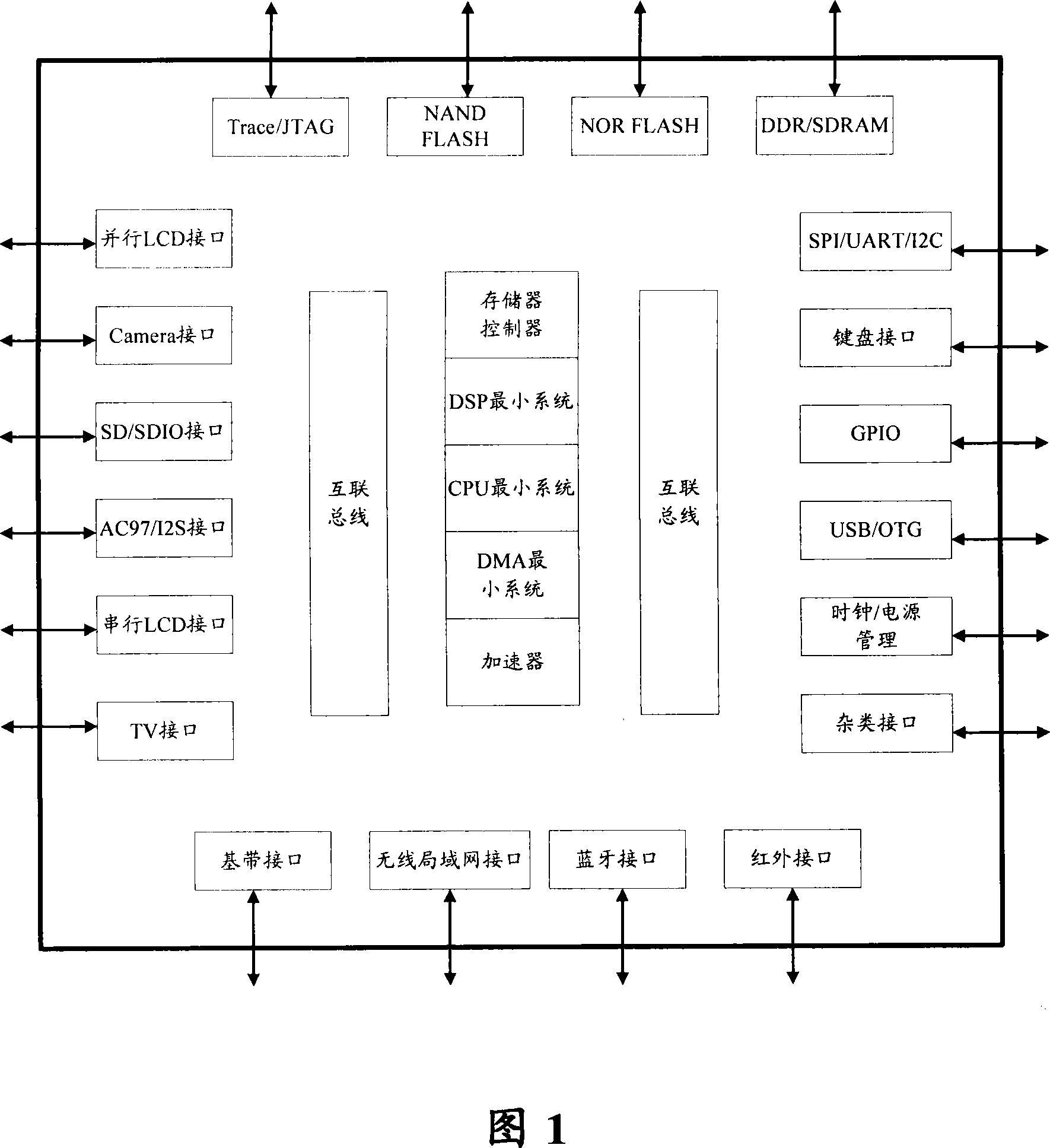
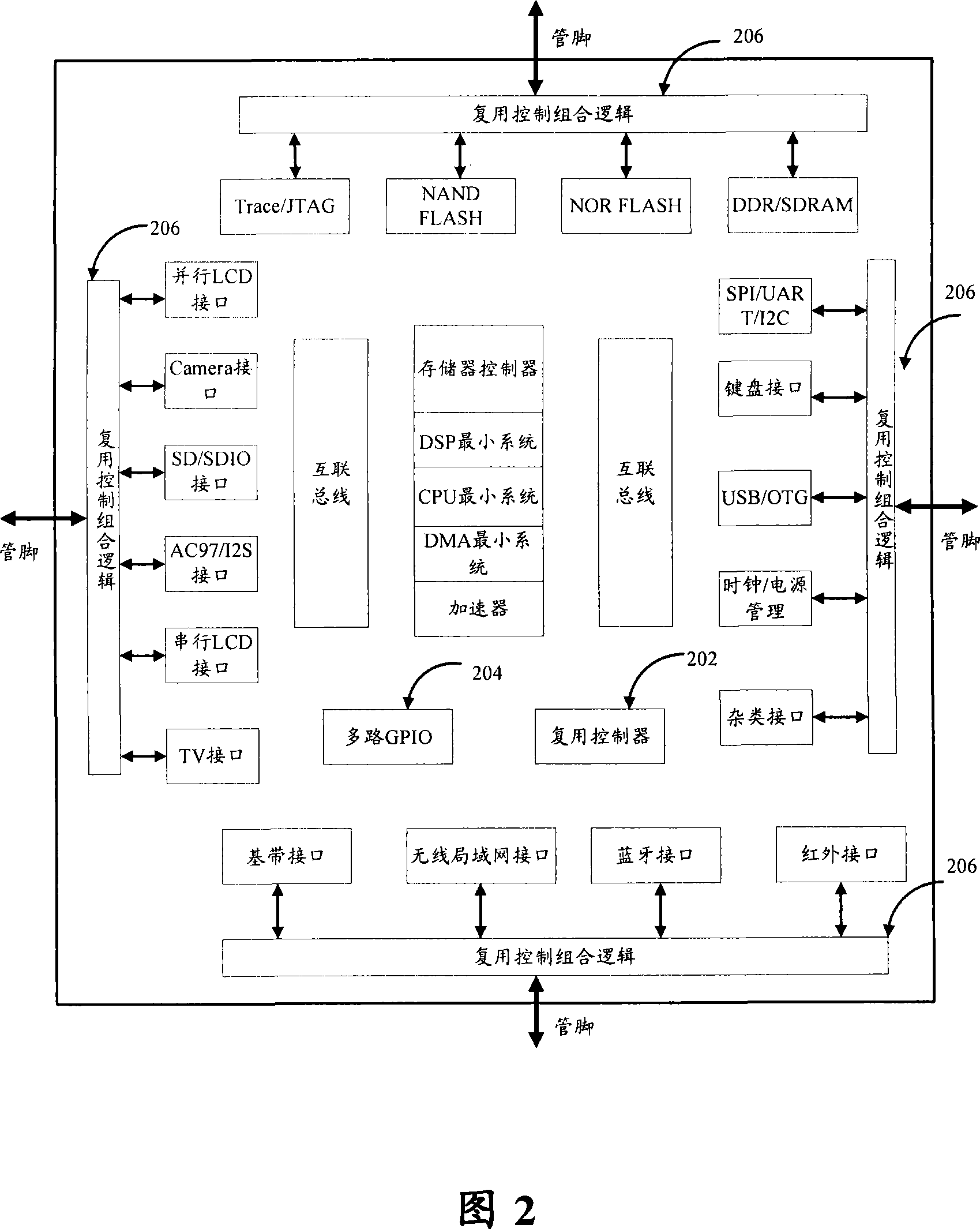
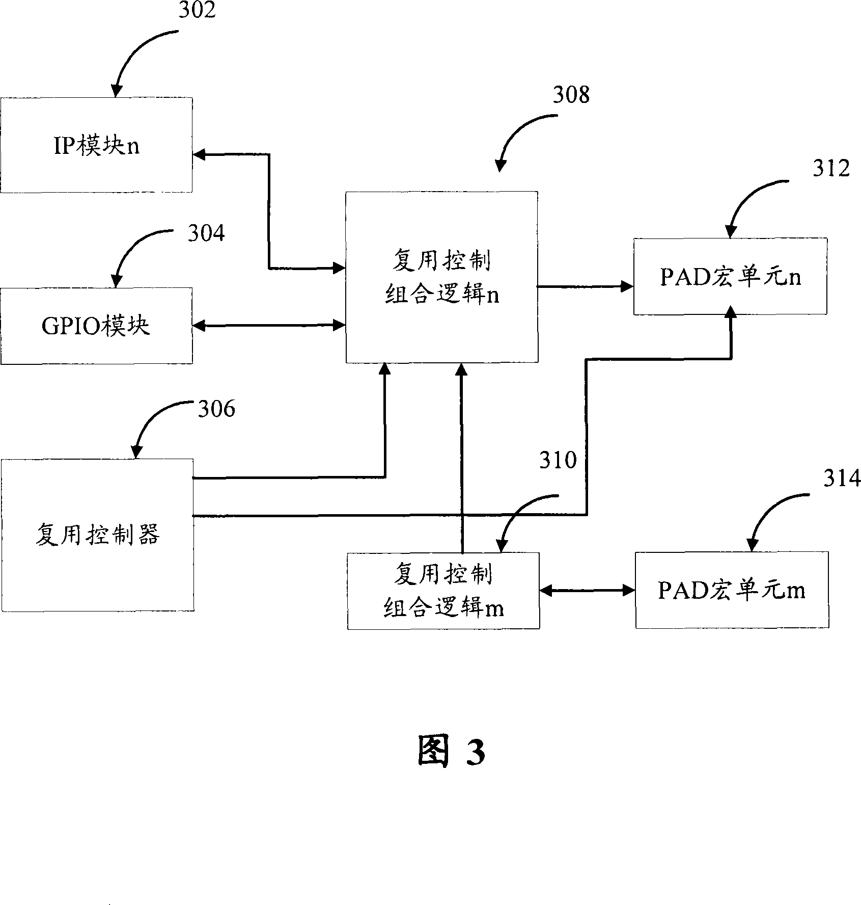
[0039] FIG. 2 is a functional block diagram showing a terminal SOC chip according to the present invention. Referring to FIG. 2, the terminal pin multiplexing device 200 according to the present invention includes: a multiplexing control module 202, which is used to control the switching between the functional module and the general I / O interface module, and to control the function module and the general I / O interface The direction of the signal of the module; and the general I / O interface module 204, which is used to determine the signal direction of the general I / O interface module, output the CPU configuration level to the multiplexing pin, and read the signal of the multiplexing pin, wherein , each multiplexing control combinatorial logic module corresponds to one multiplexing pin.

[0040] The device also includes: a plurality of multiplexing con...


PUM


Abstract

The method comprises: a multiplexing control module used for controlling the switching between the functional module and general I / O interface module, and controlling the signal direction of the functional module and general I / O interface module; and a general I / O interface module used for controlling the signal direction of the I / O interface module and outputting CPU configuration level to multiplex pins, and reading the signal of the multiplex pin. Wherein, each multiplexing control combination logic module corresponds to a multiplexing pin.

Description

technical field [0001] The invention relates to the design of a terminal SOC (system on chip) chip or a mobile phone multimedia chip, in particular to a pin multiplexing device for a super large-scale chip. Background technique [0002] With the rapid development of microelectronics and communication technology, the integration scale of chips is getting larger and larger. Terminal SOC (system on chip) chip is a typical example. Early terminal chips may require multiple chips to complete the corresponding functions, but now a terminal SOC chip integrates all functions of the baseband, and also has rich multimedia and application functions. These terminal chips include mobile phone baseband chips, mobile phone application processors, terminal multimedia processors, and multimedia player SOC chips. [0003] With the rapid growth of application requirements, terminal chip integration functions are becoming more and more abundant, such as supporting multiple memory types, suppo...

Claims


Application Information

Patent Timeline
Patent Type & Authority Applications(China)
IPC IPC(8): G06F13/40
Inventor 李树宏
Owner ZTE CORP
Why Eureka
Try Eureka