Surface light source device having secondary electron emission layer, method of manufacturing the same, and backlight unit having the same

A technology of secondary electron emission and electron emission layer, applied in the field of surface light source devices, can solve the problems of dark area, poor brightness uniformity, long brightness stabilization time, etc., and achieve reduced ignition voltage, reduced heat generation, discharge Efficiency improvement effect

A technology of secondary electron emission and electron emission layer, applied in the field of surface light source devices, can solve the problems of dark area, poor brightness uniformity, long brightness stabilization time, etc., and achieve reduced ignition voltage, reduced heat generation, discharge Efficiency improvement effect

CN101137256AInactive Publication Date: 2008-03-05SAMSUNG CORNING CO LTD

Image

  • Surface light source device having secondary electron emission layer, method of manufacturing the same, and backlight unit having the same
  • Surface light source device having secondary electron emission layer, method of manufacturing the same, and backlight unit having the same
  • Surface light source device having secondary electron emission layer, method of manufacturing the same, and backlight unit having the same

Examples


Embodiment Construction

[0040] The present invention is further fully described hereinafter with reference to the accompanying drawings, in which preferred embodiments of the invention are shown.

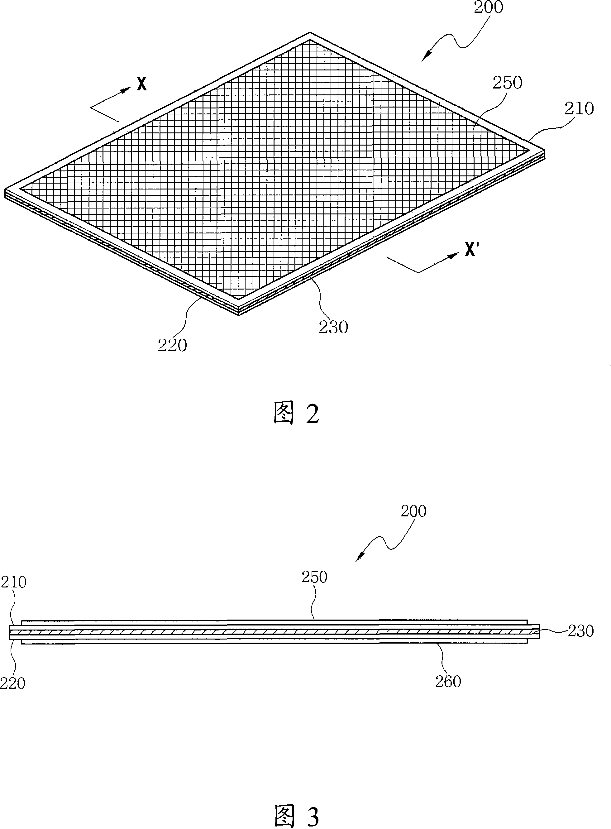
[0041] FIG. 2 is a perspective view of a surface light source device 200 according to an embodiment of the present invention, and FIG. 3 is a side view of the surface light source device 200 in FIG. 2 .

[0042] The surface light source device 200 includes a first flat substrate 210 and a second flat substrate 220 having the same shape. Preferably, the first substrate 210 and the second substrate 220 are transparent thin glass substrates. There is no limit to the thickness of the first substrate 210 and the second substrate 220, but the first substrate 210 and the second substrate have a thickness of about 1mm to 2mm, preferably 1mm or less.

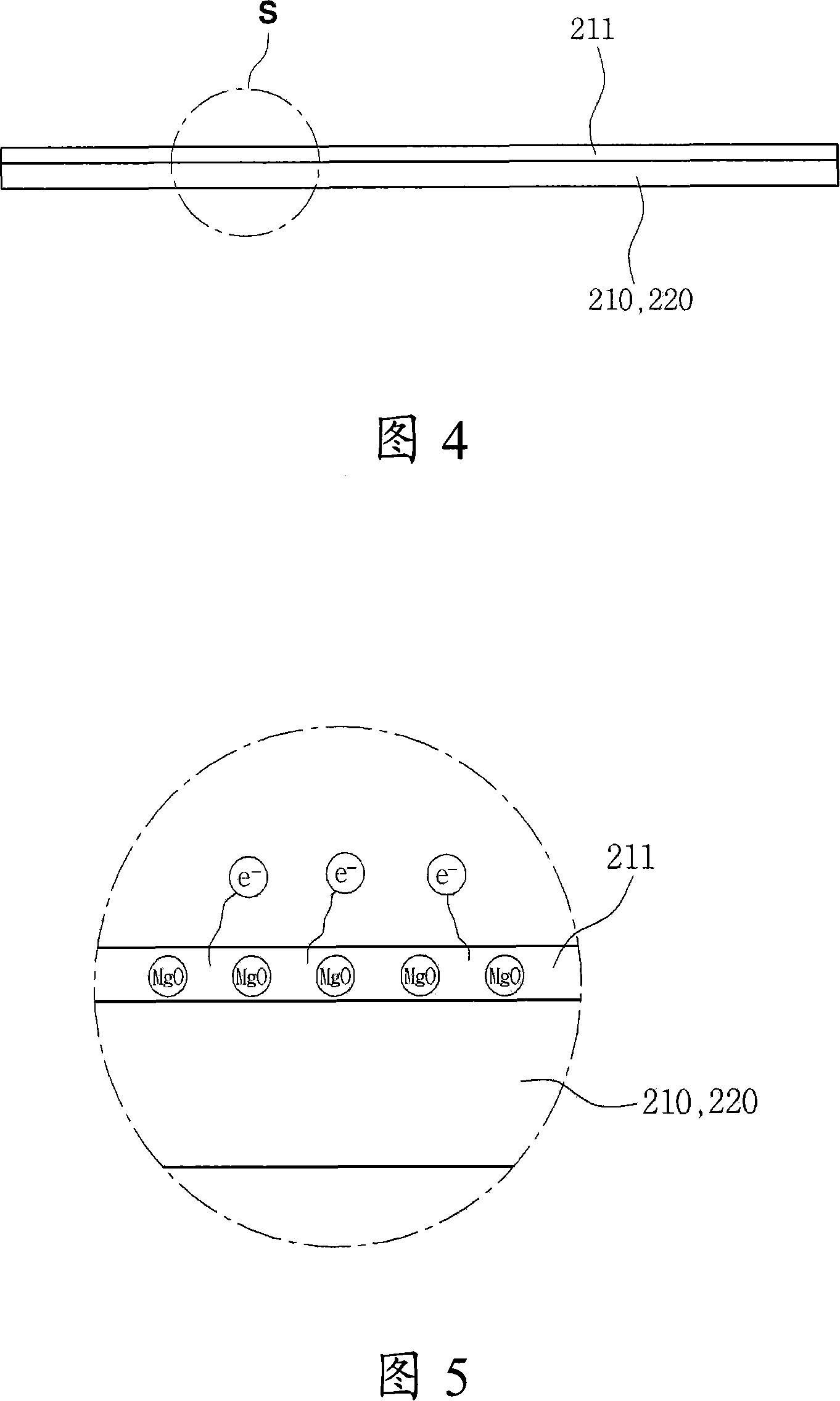
[0043] A phosphor layer is coated on inner surfaces of the first substrate 210 and the second substrate 220 , and a reflective layer may be further formed on one of...


PUM

PropertyMeasurementUnit
particle diameteraaaaaaaaaa

Abstract

There is provided a substrate for a surface light source device, comprising a first secondary electron emission layer including crystalline magnesium oxide (MgO) powder on a surface of the substrate. There is also provided a surface light source device comprising a first substrate and a second substrate facing each other at a predetermined distance between which a discharge space is formed; and an electrode to apply a discharge voltage to the discharge space, wherein a first secondary electron emission layer including crystalline MgO powder is formed on a surface of at least one of the first substrate and the second substrate. Preferably, the crystalline MgO powder is obtained by grinding an MgO sputtering target. There is provided a backlight unit comprising a surface light source device including a discharge space formed between a first substrate and a second substrate, an electrode to apply a discharge voltage to the discharge space, and a first secondary electron emission layer including crystalline MgO powder on a surface of at least one of the first substrate and the second substrate; a case to receive the surface light source device; and an inverter to supply a discharge voltage to the electrode. Preferably, a second secondary electron emission layer ion-exchanged with a secondary electron emitting material is formed under a surface of the substrate.

Description

[0001] Cross References to Related Applications [0002] This application claims the benefit of Korean Patent Application No. 2006-0083095 filed on Aug. 30, 2006, the entire disclosure of which is hereby incorporated by reference. technical field [0003] The present invention relates to a surface light source device, a method for manufacturing the surface light source device, and a backlight unit with the surface light source device, in particular to a surface light source device with a secondary electron emission layer with excellent secondary electron emission capability. Background technique [0004] Liquid crystal display (LCD) devices display images using electrical and optical properties of liquid crystals. Since LCD devices are small in size and light in weight compared to cathode ray tube (CRT) devices, they are widely used in portable computers, communication devices, liquid crystal television (LCTV) receivers, aerospace industries, and the like. [0005] The LCD ...

Claims


Application Information

Patent Timeline
05 Mar 2008
Publication
CN101137256A
IPC
H05B33/14; H05B33/12; H05B33/10; G02F1/13357; G02F1/1335
CPC
G02F1/133604; H01J11/40; H01J61/305; H01J61/35; H01J2211/40
Inventors
郑京泽; 李起渊