
Plasma display panel without transparent electrode structure and methods for manufacturing upper substrate thereof

A plasma display and transparent electrode technology, applied in the direction of AC plasma display panels, electrode system manufacturing, discharge tube/lamp manufacturing, etc., can solve problems such as glass yellowing, affecting visual effects, silver electrode design difficulties, etc., to achieve structural Fine, anti-yellowing effect

Inactive Publication Date: 2010-03-31
四川世纪双虹显示器件份有限公司
View PDF0 Cites 2 Cited by
  • Summary
  • Abstract
  • Description
  • Claims
  • Application Information

AI Technical Summary

Problems solved by technology

The inventors have found that reducing the transparent electrode will help reduce the overall manufacturing cost. However, the adverse effect of reducing the transparent electrode layer is that if the bus electrode, that is, the silver electrode, is in direct contact with the upper substrate glass, it will cause the glass to turn yellow. , which affects the visual effect
[0008] In addition, when reducing transparent electrodes, how to design corresponding silver electrodes has also become a design difficulty

Method used


Image

  • Plasma display panel without transparent electrode structure and methods for manufacturing upper substrate thereof
  • Plasma display panel without transparent electrode structure and methods for manufacturing upper substrate thereof
  • Plasma display panel without transparent electrode structure and methods for manufacturing upper substrate thereof

Examples


Embodiment Construction

[0031] The present invention will be described below with reference to the drawings and various embodiments, wherein, in each embodiment, the reference numerals of the same components are different.

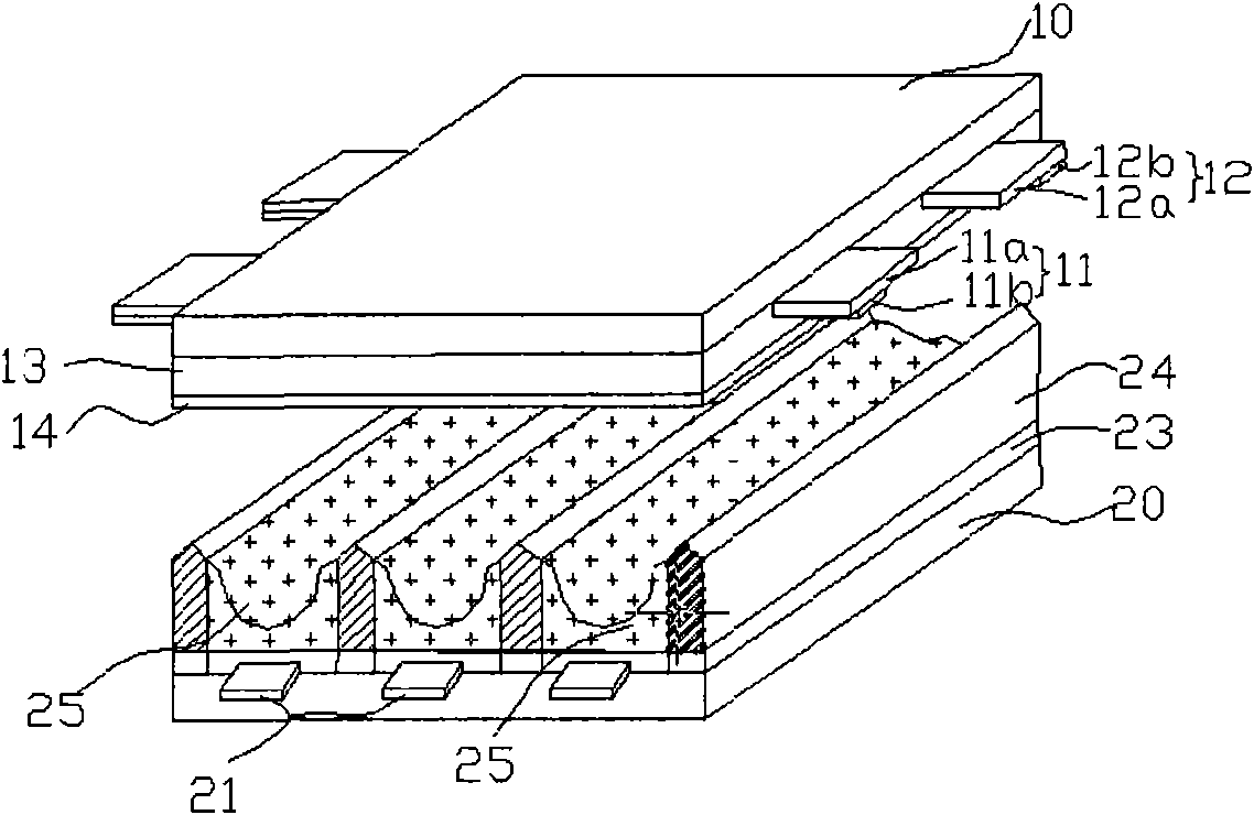
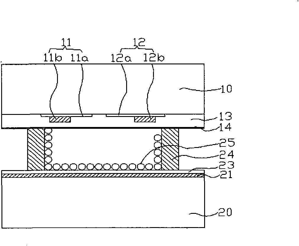
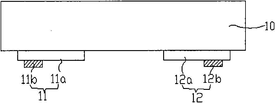
[0032] Figure 4 A schematic plan view showing an ITO-free electrode of a substrate on a plasma display panel according to the present invention. As shown in the figure, there is a first layer of magnesium oxide layer 15 on the upper substrate 10, a silver electrode 11 (silver electrode X) and a silver electrode 12 (silver electrode Y) positioned on the surface of the magnesium oxide layer, formed on the silver electrode 11 and A dielectric layer 13 on the surface of the silver electrode 12 and a second magnesium oxide layer 14 on the surface of the dielectric layer 13 . Wherein, the thickness of the first magnesium oxide layer is 1500 angstroms to 2000 angstroms.

[0033] Figure 5 A schematic plan view showing an ITO-free electrode of a substrate on a plasma display panel ac...


PUM

PropertyMeasurementUnit
Thicknessaaaaaaaaaa

Abstract

The invention discloses a plasma display panel without a transparent electrode structure, which comprises an upper substrate and a lower substrate sealed with the upper substrate, wherein the upper substrate is provided with a first magnesium oxide layer positioned on the surface of upper substrate glass, a silver electrode X and a silver electrode Y which are positioned on the surface of the magnesium oxide layer, a dielectric layer positioned on the surfaces of the silver electrode X and the silver electrode Y, and a second magnesium oxide layer positioned on the surface of the dielectric layer. The invention also discloses two methods for manufacturing the plasma display panel without the transparent electrode structure, namely an electron beam evaporation method and a magnetron sputtering method. The manufacturing cost is reduced and the brightness is increased.

Description

technical field [0001] The invention belongs to the field of gas discharge, and in particular relates to a plasma display screen without a transparent electrode structure and a method for manufacturing the upper substrate thereof. Background technique [0002] At present, the general-purpose AC gas discharge plasma display adopts a surface discharge structure, which includes an upper substrate and a lower substrate sealed together with it. The upper substrate is equipped with transparent electrodes ITO and bus electrodes, transparent electrodes and bus electrodes. Discharge electrodes are formed, and the discharge electrodes include sustain discharge electrodes X and scan discharge electrodes Y. A dielectric layer is covered on the surface of the discharge electrode, and a magnesium oxide protective layer is covered on the dielectric layer. The lower substrate is provided with addressing electrodes perpendicular to the discharge electrodes. The addressing electrodes are cov...

Claims


Application Information

Patent Timeline
IPC IPC(8): H01J17/49H01J17/02H01J17/04H01J9/00H01J9/02H01J11/10H01J11/40
Inventor 曹瑞林
Owner 四川世纪双虹显示器件份有限公司
Learn More