
Plasma display panel device and drive method thereof

a technology of display panel and plasma, which is applied in the direction of instruments, static indicating devices, etc., can solve problems such as image deterioration, and achieve the effects of reducing the cost of the whole device, reducing the firing voltage, and effectively restricting the generation of erroneous discharges

Inactive Publication Date: 2009-01-08
PANASONIC CORP
View PDF16 Cites 2 Cited by
  • Summary
  • Abstract
  • Description
  • Claims
  • Application Information

AI Technical Summary

Benefits of technology

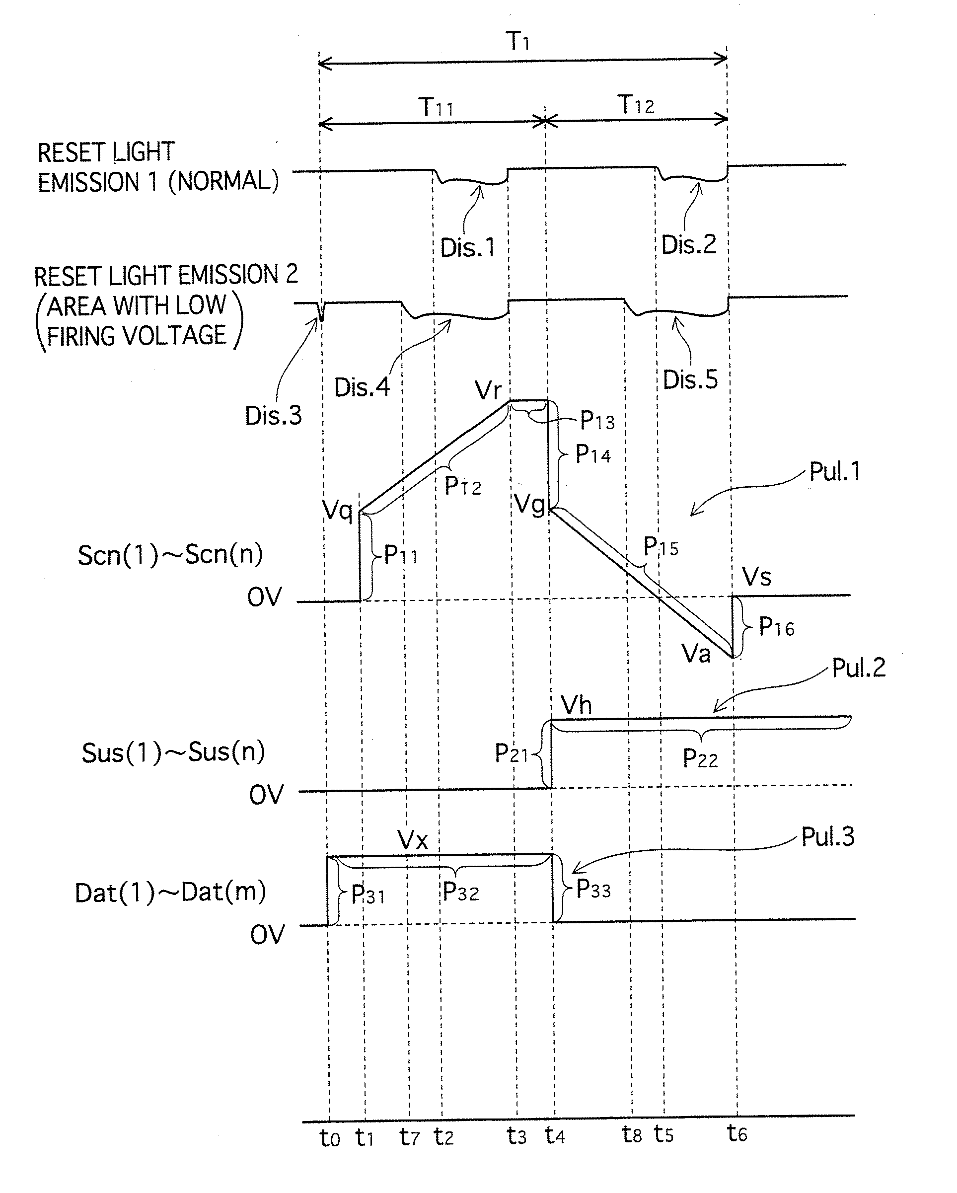
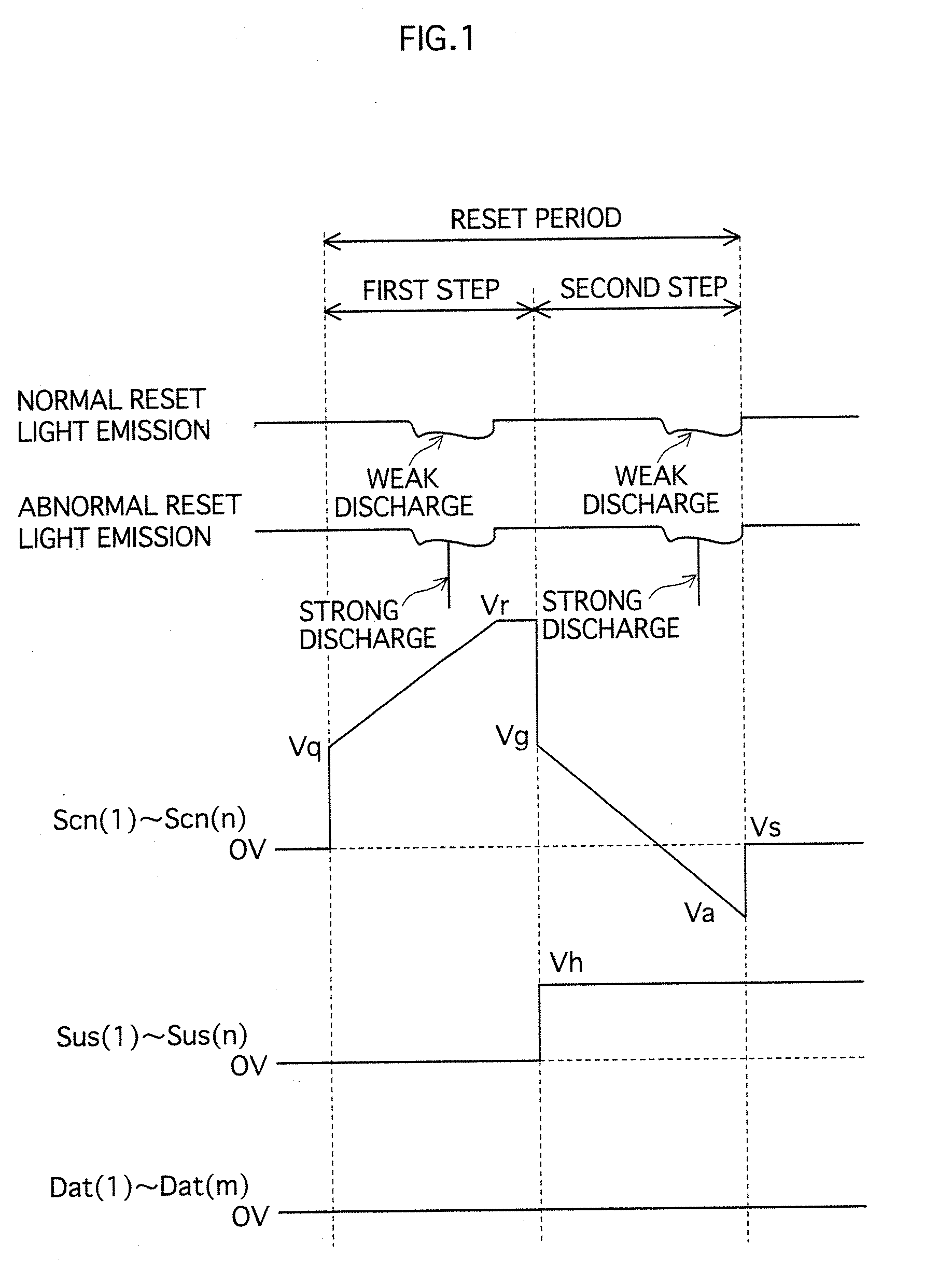
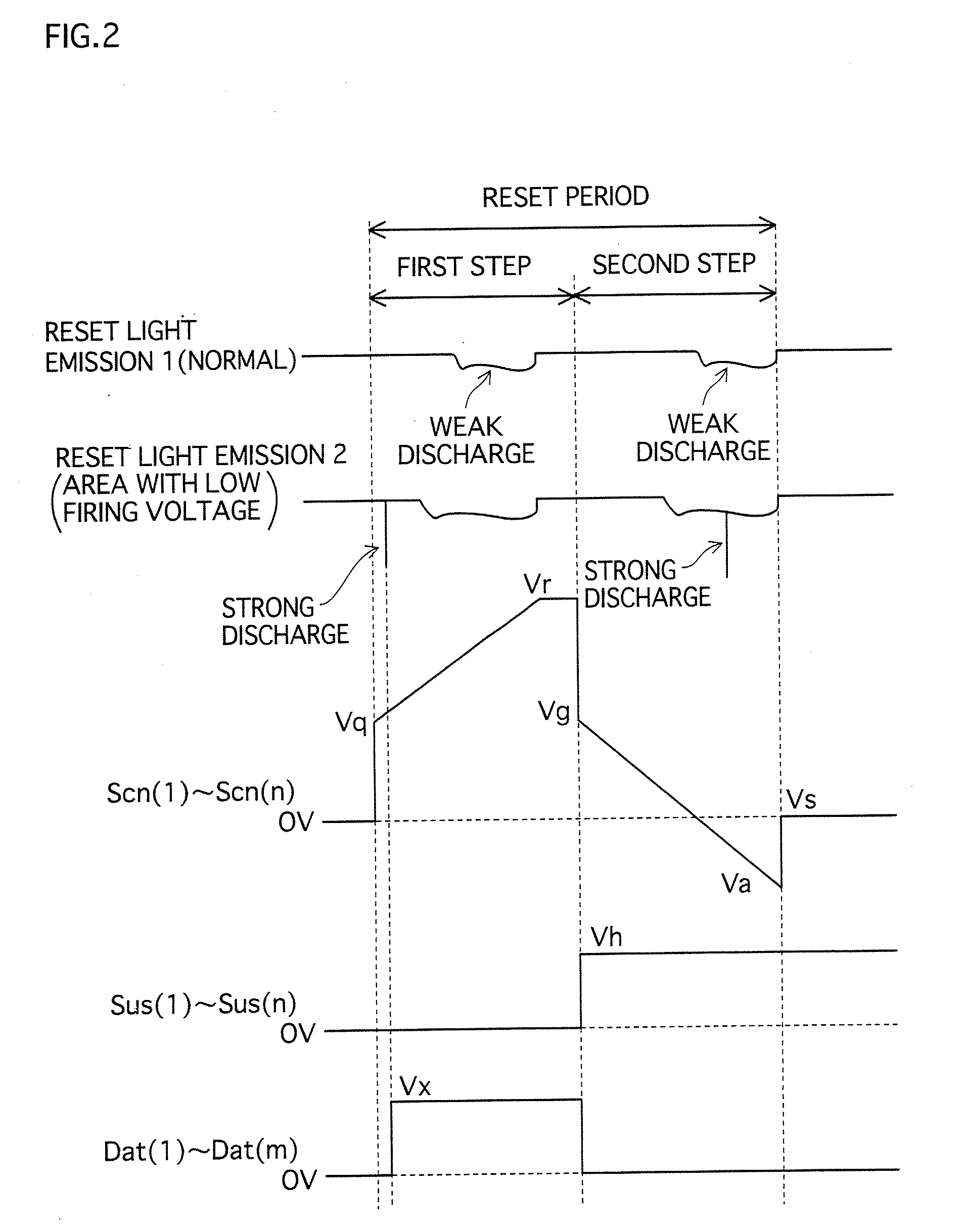
[0022]In the PDP device and the drive method thereof of the present invention, a voltage having a waveform of a positive polarity relative to second electrodes is applied to the third electrodes in the period first step at a timing prior to generation of the first reset discharge. With this construction of the PDP device and the drive method thereof of the present invention, even if some areas have a lower firing voltage than the other areas due to variation of a property in the panel surfaces, a discharge that is strong enough to influence the address period and the sustain period is not generated in the period first step of the all-cell reset period. More specifically, any of the above-described two methods (1) and (2) and a combination of the methods may be adopted.
[0023]When, for example, the above-described method (1) is adopted, a ramp waveform is applied to the rising portion. With this construction, if a discharge is generated between the third electrodes and the second electrodes by a voltage applied to the third electrodes, the generated discharge is only a weak discharge and does not extend to the first electrodes side. As a result, the method of the present invention can effectively restrict the generation of a discharge that is strong enough to extend to the first electrodes in the period first step in the all-cell reset period and to influence the address period. Accordingly, with the adoption of the method of the present invention, even if panel surfaces include some areas that have a lower firing voltage than the other areas due to variation of a property in the panel surfaces or due to a long-term driving, it is possible to effectively restrict the generation of an erroneous discharge in the all-cell reset period. It should be noted here that the ramp waveform is described in detail in “ASIA DISPLAY '98, pp. 23-27” and the like, and the slant of the waveform is described in detail in Japanese Patent Publication No. 3394010 (for example, 9V / μ sec.) and the like, and that description of these terms is omitted here.
[0024]The above-described method (1) makes it possible to restrict the generation of an erroneous discharge if the application of the voltage to the third electrodes in the period first step is performed at the same time of after the application of the voltage to the first electrodes. This construction produces an advantageous effect of eliminating the need to ensure an excessive amount of withstanding voltage for the address driver in relation to the wringing by the potential change in the third electrodes, as well as the effect of restricting the generation of an erroneous discharge in the all-cell reset period. Accordingly, with the adoption of the present method, it is possible to reduce the cost for the whole device cost as a whole.
[0025]In the above-described method (1), it is preferable, in terms of restricting the generation of an erroneous discharge, that a slant of the rising ramp waveform portion in the waveform of the voltage applied to the third electrodes in the period first step is set to be slower than a slant of a rising portion in a waveform of the voltage applied to the third electrodes in the address period.
[0026]When the above-described method (2) is adopted, a voltage is applied to the third electrodes at a timing prior to a timing when a voltage starts to be applied to the first electrodes. With this construction, if a discharge is generated between the third electrodes and the second electrodes by a voltage applied to the third electrodes, since there is no potential difference between the first electrodes and the second electrodes at the time when the discharge is generated, the discharge does not become a trigger for developing into a strong discharge. Accordingly, with the adoption of the present method, even if panel surfaces include some areas that have a lower firing voltage than the other areas due to variation of a property in the panel surfaces or due to a long-term driving, it is possible to restrict the generation of an erroneous discharge in the all-cell reset period.
[0027]In the above-described method (2), it is preferable that the timing at which the rising ramp waveform portion in the waveform of the voltage applied to the third electrodes starts is set with a predetermined time period before the timing at which the rising portion in the waveform of the voltage applied to the first electrodes starts such that even if a discharge is generated between the third electrodes and the second electrodes by the application of the voltage to the third electrodes, an influence of the discharge generated between the third electrodes and the second electrodes attenuates within the predetermined time period.

Problems solved by technology

The wall discharge generated here resembles a wall discharge that is generated when an addressing is made, and thus leads to deterioration of images.

Method used


Image

  • Plasma display panel device and drive method thereof
  • Plasma display panel device and drive method thereof
  • Plasma display panel device and drive method thereof

Examples


embodiment 1

1. Construction of Panel 10

[0071]Here, among the constituent elements of a PDP device 1 in Embodiment 1 of the present invention, the construction of a panel unit 10 will be described first, with reference to FIG. 3. FIG. 3 is a main part perspective view (partially sectional view) showing the construction of the panel unit 10 in Embodiment 1.

1-1. Construction of Front Panel 11

[0072]A front panel 11 is constructed such that a plurality of display electrode pairs 112, each pair being made of scan electrode Scn and sustain electrode Sus, are disposed in parallel with each other on a surface (in FIG. 3, the lower surface) of a front substrate 111 that faces a back panel 12. And a dielectric layer 113 and a protective layer 114 are formed to cover the display electrode pairs 112, in the stated order.

[0073]The front substrate 111 is made of, for example, a high-strain-point glass or a soda-lime glass. Each scan electrode Scn is a stack of a transparent electrode portion 1121 and a bus el...

embodiment 2

[0158]A drive method of a PDP device in Embodiment 2 will be described with reference to FIG. 10. FIG. 10 is a waveform diagram showing waveforms of the voltages applied to the scan electrodes Scn(1)-Scn(n), the sustain electrodes Sus(1)-Sus(n), and the address electrodes Dat(1)-Dat(m) during the all-cell reset period T5, corresponding to a part of the drive method of the PDP device in Embodiment 2.

[0159]The PDP device of the present embodiment has the same construction as the PDP device 1 in Embodiment 1, and the drive method of the present embodiment is the same as the method shown in FIG. 5 of Embodiment 1, except for the all-cell reset period T5. Therefore, most of the description of the device and method is omitted here, and the following description will focus on the all-cell reset period T5.

[0160]As shown in FIG. 10, in the drive method of the present embodiment, the pulses Pul.1 and Pul.2, which are respectively applied to the scan electrodes Scn(1)-Scn(n) and to the sustain...


PUM


Abstract

Provided are a PDP device and a drive method thereof which restrict the generation of an erroneous discharge in the all-cell reset period and to restrict the appearance of flickers in the areas with low grayscale levels even if some areas have a lower firing voltage than the other areas due to variation of a property in the panel surfaces or due to a long-term driving, or even if the voltage applied to the address electrode is increased with the pursuit of high definition.The pulse Pul.3 is applied to address electrodes Dat at timing t0 prior to timing t1 when the potential of the scan electrodes Scn is increased to Vq(V). In this drive method, voltage Vx(V) is applied to address electrodes Dat so that there is no potential difference between the scan electrodes Scn and the sustain electrodes Sus at timing t0 when discharge Dis.3 is generated. Accordingly, the discharge Dis.3, which is generated between the scan electrodes Scn and the sustain electrodes Sus due to reduction in the firing voltage, does not become a trigger for extending to the scan electrodes Scn to generate an erroneous discharge.

Description

TECHNICAL FIELD[0001]The present invention relates to a plasma display panel device and a drive method thereof, and specifically relates to a technology for restricting an erroneous discharge from occurring during a reset period when the device is driven.BACKGROUND ART[0002]Plasma display panels (hereinafter referred to as PDPs), especially the AC surface-discharge type PDPs, have a construction in which two panels are arranged to face each other with a space therebetween, are sealed at the perimeter, and a discharge gas containing xenon (Xe) and others are filled in the inner space of the sealed panels. One of the two panels (front panel) has a construction in which a plurality of pairs of display electrodes are formed on a main surface of a glass substrate, and a dielectric layer and a protective layer are formed to cover the display electrodes, in the stated order.[0003]The other panel (back panel) has a construction in which a plurality of address electrodes are formed on a main...

Claims


Application Information

Patent Timeline
Patent Type & Authority Applications(United States)
IPC IPC(8): G09G3/28
CPCG09G3/2927G09G2320/0247G09G2320/0238G09G2310/066
Inventor AKAMATSU, KEIJIOGAWA, KENJIUEDA, MITSUO
Owner PANASONIC CORP
Learn More