Magnetoresistive element and magnetic memory
一种磁阻元件、元件的技术,应用在静态存储器、数字存储器信息、磁场控制的电阻器等方向,能够解决难以供给磁场等问题
- Summary
- Abstract
- Description
- Claims
- Application Information
AI Technical Summary
Problems solved by technology
Method used
Image
Examples
no. 1 example
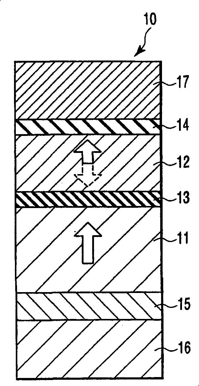
[0058] figure 1 is a sectional view showing the structure of the MTJ element 10 according to the first embodiment. figure 1 The arrows in indicate the direction of magnetization. In this embodiment, an MTJ element 10 having a single pinned layer structure (ie, a structure in which a free layer and a pinned layer are arranged on both sides of a nonmagnetic layer) will be described.
[0059] The MTJ element 10 has a crystal orientation lower layer 15, a pinned layer (also called a magnetization pinned layer or pinned layer) 11, a tunnel barrier layer (nonmagnetic layer) 13, a recording layer (also called a magnetization free layer or A layered structure formed by a free layer) 12 and a capping layer 14. The layered structure may have a reverse stacking order. Lower electrode 16 is provided on the lower surface of crystal orientation lower layer 15 . The upper electrode 17 is provided on the upper surface of the cap layer 14 .
[0060] The pinned layer 11 has a fixed magneti...
no. 2 example
[0116] In the second embodiment, a magnetic layer for controlling the crystallinity of the tunnel barrier layer 13 is inserted between the tunnel barrier layer 13 and the pinned layer 11 , thereby increasing the crystallinity of the tunnel barrier layer 13 and the recording layer 12 .
[0117] Figure 4 is a sectional view showing the structure of the MTJ element 10 according to the second embodiment. In this embodiment, an MTJ element 10 having a single pinned layer structure will be explained.
[0118] The MTJ element 10 has a layered structure formed by sequentially stacking a crystal orientation lower layer 15 , a pinned layer 11A, an interface pinned layer 11B, a tunnel barrier layer 13 , a recording layer 12 , and a cap layer 14 . Layered structures may have a reverse stacking order. Lower electrode 16 is provided on the lower surface of crystal orientation lower layer 15 . The upper electrode 17 is provided on the upper surface of the cap layer 14 .
[0119] The fix...
no. 3 example
[0122] In the third embodiment, a magnetic layer for enhancing the magnetoresistance effect is inserted between the recording layer 12 and the tunnel barrier layer 13, thereby improving the characteristics of the MTJ element 10.
[0123] Figure 5 is a sectional view showing the structure of the MTJ element 10 according to the third embodiment. In this embodiment, an MTJ element 10 having a single pinned layer structure will be explained.
[0124] The MTJ element 10 has a layered structure formed by sequentially stacking a crystal orientation lower layer 15 , a fixed layer 11 , a tunnel barrier layer 13 , an interface recording layer 12B, a recording layer 12A, and a capping layer 14 . Layered structures may have a reverse stacking order. Lower electrode 16 is provided on the lower surface of crystal orientation lower layer 15 . The upper electrode 17 is provided on the upper surface of the cap layer 14 .
[0125] The recording layer 12 of this embodiment is formed by lami...
PUM
 Abstract
Description
Claims
Application Information


