PCBConnection method for implementing common use of single and double density in PCB test
A double-density, wiring technology, applied in the direction of electronic circuit testing, components of electrical measuring instruments, measuring electricity, etc., can solve the problem of rising PCB testing costs and achieve the effect of reducing costs
- Summary
- Abstract
- Description
- Claims
- Application Information
AI Technical Summary
Problems solved by technology
Method used
Image

Examples
Embodiment Construction
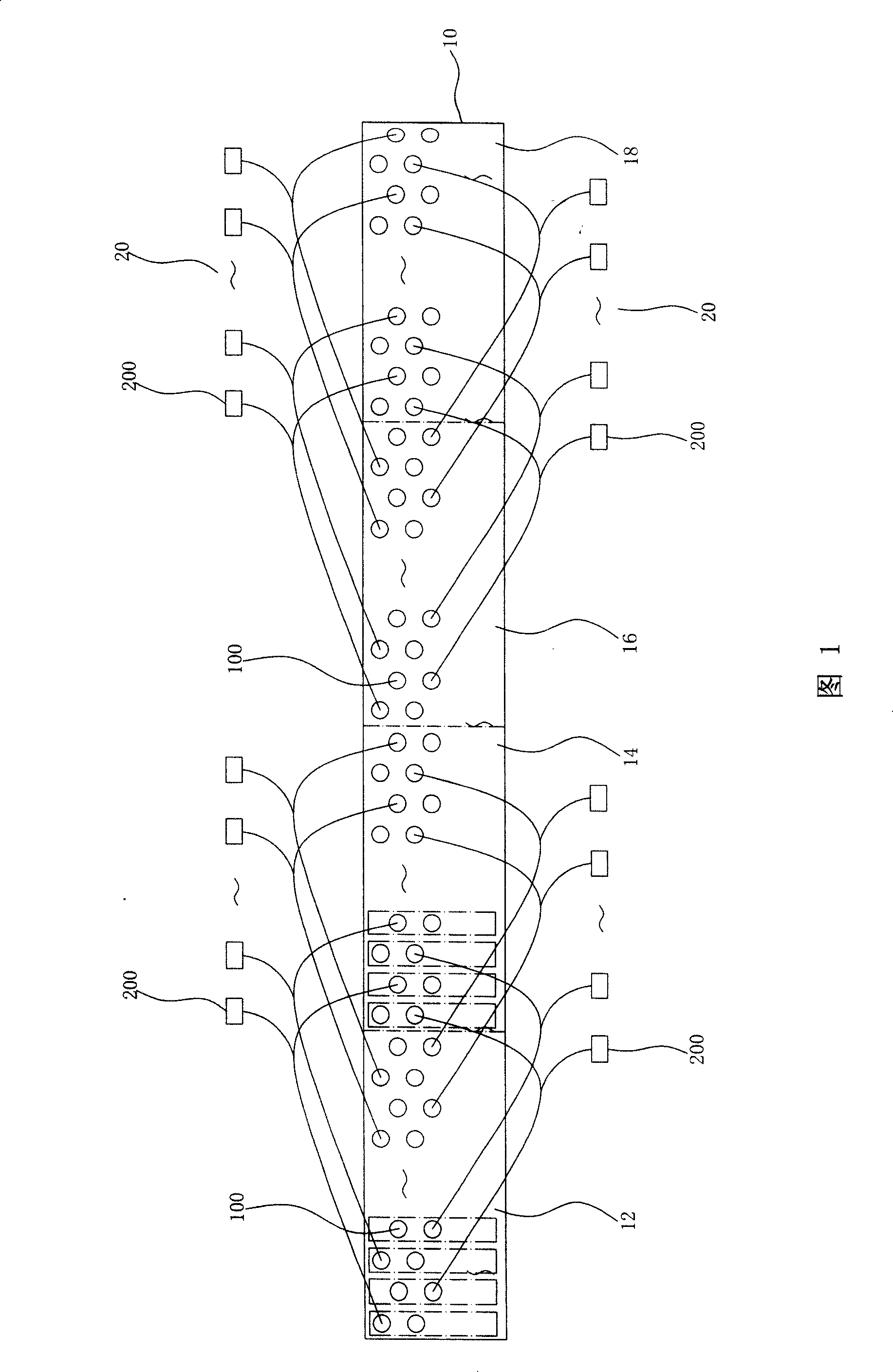
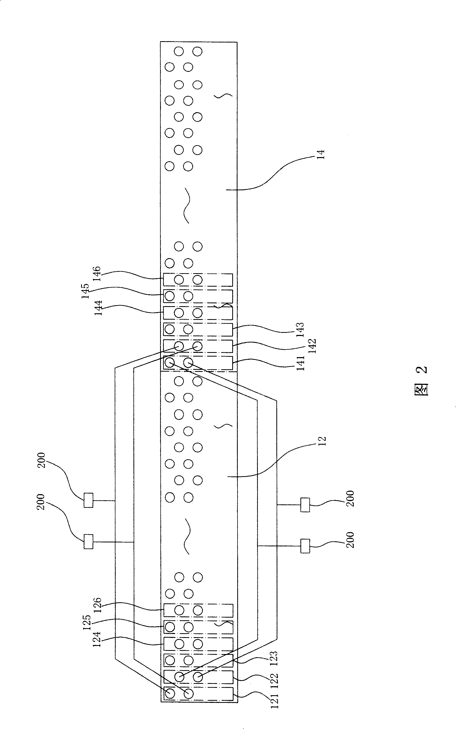
[0013] The wiring method for realizing single and double density sharing in the PCB test disclosed by the present invention is used to connect the double density grid and the single density test channel group, and can improve the existing single density testing machine, and its single density grid The grid replacement is set to a double-density grid, so that the improved single-density testing machine can perform both single-density testing and double-density testing.
[0014] With reference to Fig. 1 and shown in Fig. 2, the present invention provides a double-density grid 10 and a single-density test channel group 20, the double-density grid 10 is equally divided into a first area 12, a second area 14, and a third area 16 And the fourth area 18 and other four areas, the number of test points 100 on each area is the same. The odd-numbered test point columns on the first area 12 correspond to the even-numbered test point columns on the second area 14 in sequence, that is, the ...
PUM
 Abstract
Description
Claims
Application Information
 - R&D
- Intellectual Property
- Life Sciences
- Materials
- Tech Scout
- Unparalleled Data Quality
- Higher Quality Content
- 60% Fewer Hallucinations
Browse by: Latest US Patents, China's latest patents, Technical Efficacy Thesaurus, Application Domain, Technology Topic, Popular Technical Reports.
© 2025 PatSnap. All rights reserved.Legal|Privacy policy|Modern Slavery Act Transparency Statement|Sitemap|About US| Contact US: help@patsnap.com