A device comprising a sensor module

A sensor module and sensor technology, applied in the direction of radiation control devices, semiconductor devices, electric solid devices, etc., can solve problems such as difficulties, unfavorable devices, expensive, etc., and achieve the effects of saving packaging, low cost, and precise alignment

Inactive Publication Date: 2008-07-09
盛投资有限责任公司
View PDF1 Cites 8 Cited by
  • Summary
  • Abstract
  • Description
  • Claims
  • Application Information

AI Technical Summary

Problems solved by technology

Because of the larger functional area required, the alternative approach of using back-end processing (i.e. CMOS back-end integration) is another expensive option due to the fact that larger original substrate area is required
This difficult and complex process and the large original substrate area with large functional area make such existing devices relatively expensive during fabrication
[0006] The known device is disadvantageous, in particular due to the fact that it is relatively expensive

Method used


Image

  • A device comprising a sensor module
  • A device comprising a sensor module
  • A device comprising a sensor module

Examples


no. 1 example

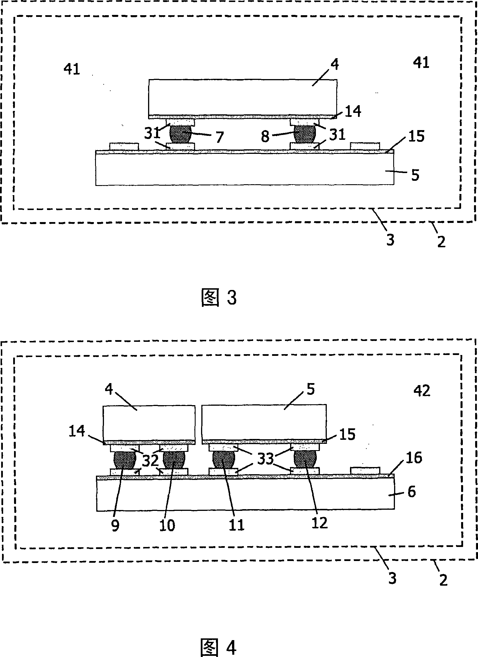
[0046] The sectional view (first option) of FIG. 3 represents a first embodiment of a sensor module according to the invention, which discloses a sensor module 2 comprising a package 3 . The package 3 comprises a first substrate 4 with a first functional layer 14 . The package 3 comprises a second substrate 5 with a second functional layer 15 . One of the functional layers 14, 15 comprises sensors not shown, while the other functional layer 14, 15 comprises active silicon which in a way provides an Application Specific Integrated Circuit (ASIC) function. A first number of pads 7 , 8 are connected to the two functional layers 14 , 15 via first bonding elements 31 , the other bonding elements being connected to leads 41 for electrical connection with a circuit not shown.

[0047] A method of monolithic integration of functional layers comprising at least one-dimensional sensors for sensing fields in at least one direction is disclosed, the sensors having an application specific...


PUM


Abstract

A device (1) comprising a sensor module (2) with a package (3) is produced at reduced costs by providing the package (3) with two or more substrates (4,5) each with a functional layer (14,15), at least one sensor (24,25) such as a magnetometer and / or an accelerometer being located in at least one functional layer (14,15), and by providing the package (3) with a system comprising solder bumps (7-12) for aligning the functional layers (14,15). The system either comprises a first number of solder bumps (7,8) for coupling the functional layers (14,15) electrically and mechanically to each other via first bonding elements (31) or comprises a third substrate (6) with a third functional layer (16) and a second number of solder bumps (9,10) for coupling the first and third functional layers (14,16) electrically and mechanically to each other via second bonding elements (32) and a third number of solder bumps (11,12) for coupling the second and third functional layers (15,16) electrically and mechanically to each other via third bonding elements (33). Mechanically and / or electrically dummy solder bumps improve the alignment of the functional layers (14,15).

Description

technical field [0001] The invention relates to a device comprising a sensor module, and also to a sensor module and a method of manufacturing the sensor module and the device. Background technique [0002] Examples of such devices are portable computers and small handheld electronic devices such as mobile phones, personal digital assistants, digital cameras and global positioning systems, and electronic devices such as aircraft, automobiles, motorboats, scooters, etc. Large transport equipment such as , mopeds and bicycles. Examples of such sensor modules are sensor modules for measuring magnetic, electric and gravitational fields. [0003] A prior art device is known as US 6,836,971 B1 which discloses a system with a sensor module comprising a first sensor (tilt sensor) and a second sensor (magnetic sensor). [0004] According to a first option, the first and the second sensor are produced separately from each other. In addition, a first substrate having a first functio...

Claims


Application Information

Patent Timeline
Patent Type & Authority Applications(China)
IPC IPC(8): H01L27/146H01L31/0203
CPCH01L27/14636H01L2924/0002H01L31/0203H01L27/14618H01L27/14634H01L2924/00H01L27/146
Inventor 汉斯·M·B·波依特尼斯·J·伊金克尼古拉斯·J·A·范费恩
Owner 盛投资有限责任公司
Why Eureka
Try Eureka