
Conductive layer structure for chip encapsulation module and its making method

A chip packaging and manufacturing method technology, applied in semiconductor/solid-state device manufacturing, circuits, electrical components, etc., can solve the problems of easy oxidation of conductive layers, achieve the effects of suppressing noise, improving EMI protection performance, and structural stability

Inactive Publication Date: 2008-08-06
XINTEC INC
View PDF0 Cites 4 Cited by
  • Summary
  • Abstract
  • Description
  • Claims
  • Application Information

AI Technical Summary

Problems solved by technology

[0007] In view of this, the main purpose of the present invention is to provide a conductive layer structure and related manufacturing method that can solve the problem of easy oxidation of the conductive layer of the chip package module, improve EMI protection performance, and effectively suppress noise

Method used


Image

  • Conductive layer structure for chip encapsulation module and its making method
  • Conductive layer structure for chip encapsulation module and its making method
  • Conductive layer structure for chip encapsulation module and its making method

Examples


Embodiment Construction

[0041] The features of the present invention can be clearly understood by referring to the accompanying drawings of this specification and the detailed description of the embodiments.

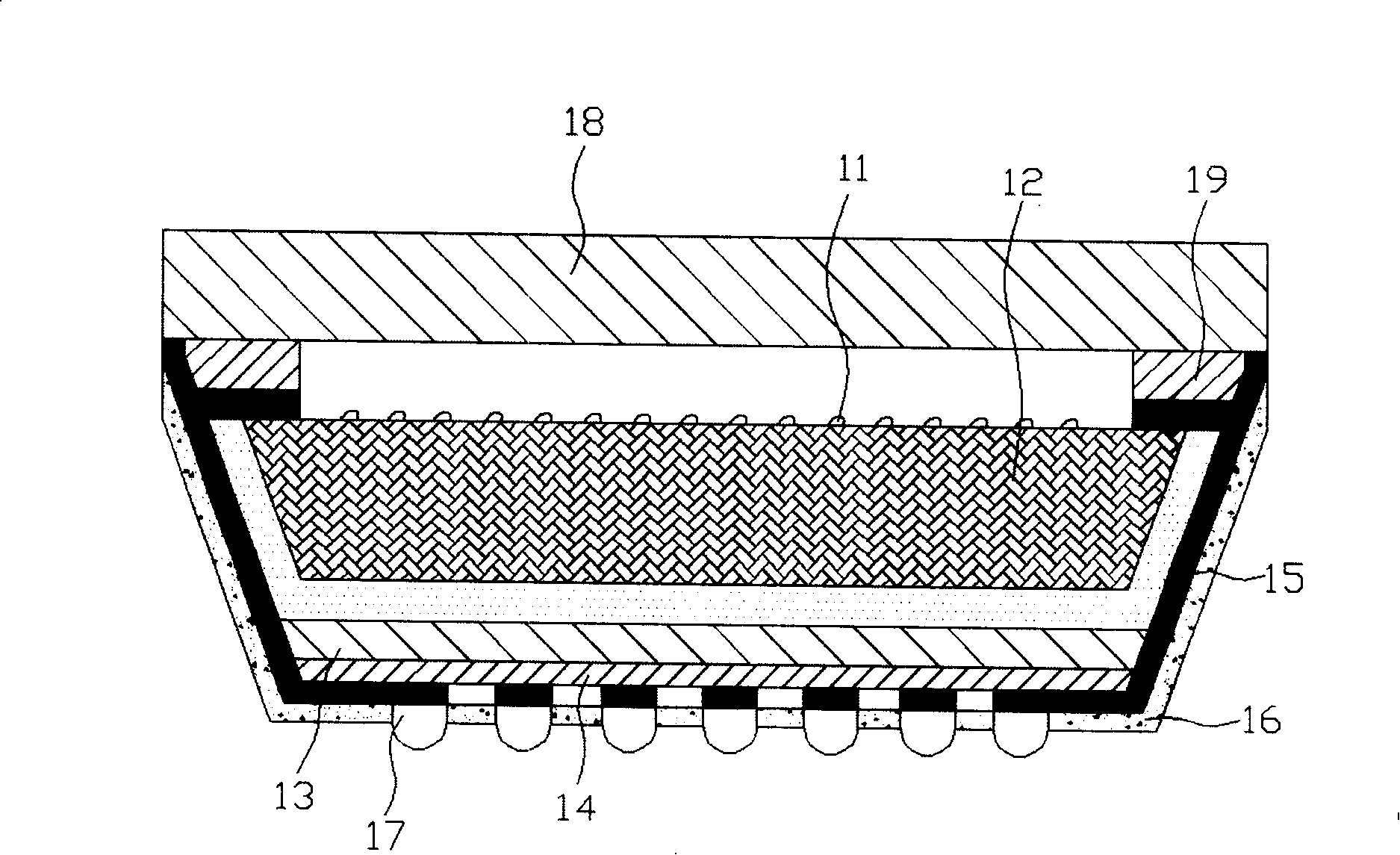
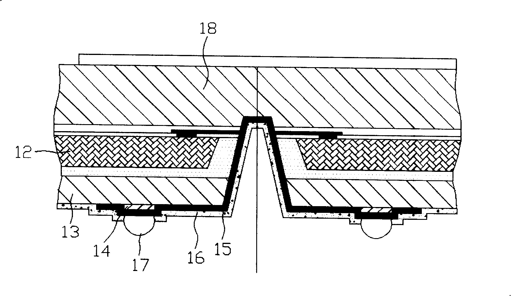
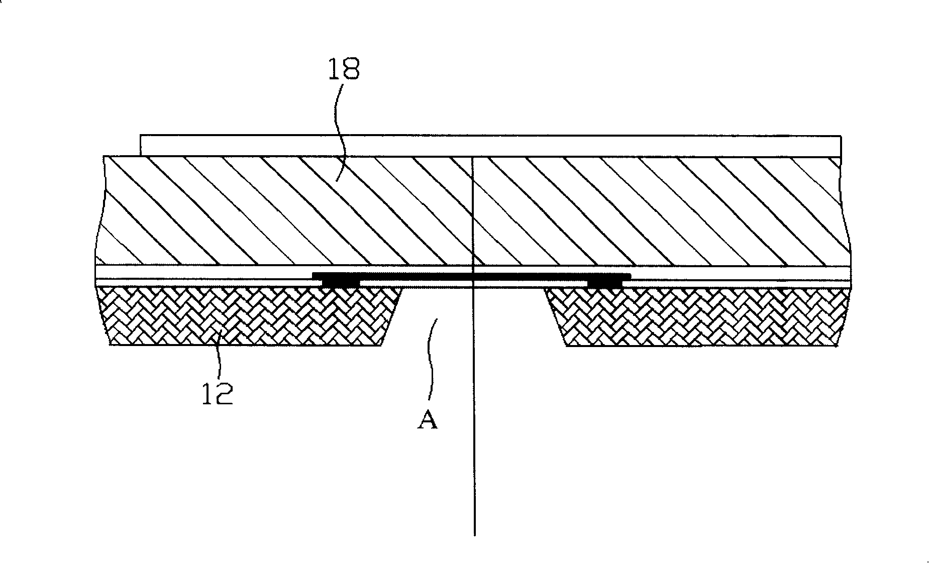
[0042] The present invention mainly solves the problems that the conductive layer of the existing chip packaging module is easy to oxidize and corrode, cannot effectively suppress noise, and the structure is unstable, such as Figure 4 (A cross-sectional view of the structure of the chip package module in a preferred embodiment of the present invention) shows that the chip package module used in the present invention also includes parts such as photosensitive chips 21, circuit structures, and housings; wherein, all photosensitive chips used for photosensitive 21 are arranged on a wafer 22 arranged inside the housing.

[0043] Wherein, an insulating layer 23, a conductive layer 24, and the outermost solder resist layer 25 and circuit pins 26 are sequentially arranged under the wafer 22; in the e...


PUM


Abstract

The invention provides a conductive layer structure on a chip packaging module and a method for manufacturing the chip packaging module. The method mainly comprising the following steps of: drilling at least one through hole to the top of a wafer at the bottom of an insulation layer of the chip packaging module, arranging insulation materials on the inner wall of each through hole to allow a conductive layer arranged at the periphery of the insulation layer to extend to the above of the wafer and then arranging a solder mask and a circuit pin so as to constitute a conductive layer structure which can be covered entirely to prevent oxidation, can enhance EMI protection performance and suppress noise effectively. The conductive layer structure not only can solve the problem that the conductive layer of the prior chip packaging module is easy to corrode due to oxidation, but also can make the conductive layer obtain better EMI shielding at the position close to other electronic elements and further enhance the EMI protection performance of the whole chip packaging module and effectively suppress the noise of the chip packaging module; meanwhile, the conductive layer structure can avoid 'T CONTACT' type contact to be more stable.

Description

technical field [0001] The invention relates to a chip packaging module, especially improving the conductive layer structure of the chip packaging module, aiming to provide a conductive layer structure that is completely covered to prevent oxidation, improve EMI protection performance and effectively suppress noise. Background technique [0002] In recent years, due to the requirements of light weight and miniaturization of electronic products, the assembly and construction technology of electronic components has gradually developed towards the goal of lightness, thinness, shortness and smallness. The capability of / O signal and current, and the function of providing heat dissipation and protecting the photosensitive chip must be packaged to form an integrated chip package module. [0003] Such as figure 1 The image sensor shown is taken as an example, which can be regarded as one of typical modular chip packaging components. Similar image sensors include photosensitive chi...

Claims


Application Information

Patent Timeline
IPC IPC(8): H01L23/552H01L23/48H01L21/50H01L21/60
CPCH01L2224/11H10K30/88
Inventor 刘建宏
Owner XINTEC INC
Learn More