Semiconductor device and method of manufacturing the same

A manufacturing method and semiconductor technology, which are applied in the fields of semiconductor/solid-state device manufacturing, semiconductor devices, electric solid-state devices, etc., to achieve the effect of improving the qualification rate and reducing the number of manufacturing processes

Inactive Publication Date: 2008-08-27
PANASONIC CORP
View PDF1 Cites 1 Cited by
  • Summary
  • Abstract
  • Description
  • Claims
  • Application Information

AI Technical Summary

Problems solved by technology

However, since the external dimensions and shapes of semiconductor elements are different for eac

Method used


Image

  • Semiconductor device and method of manufacturing the same
  • Semiconductor device and method of manufacturing the same
  • Semiconductor device and method of manufacturing the same

Examples


Embodiment Construction

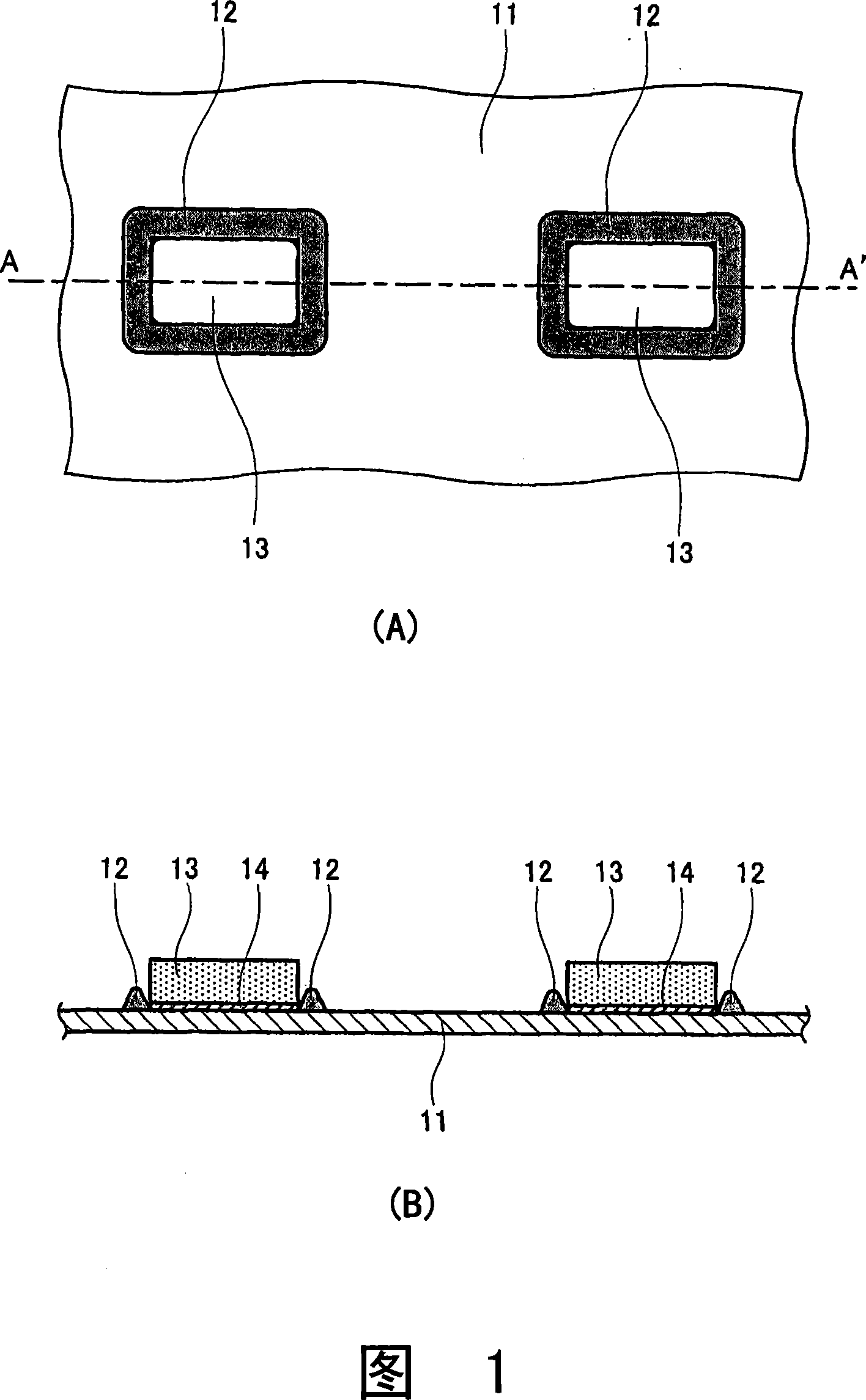
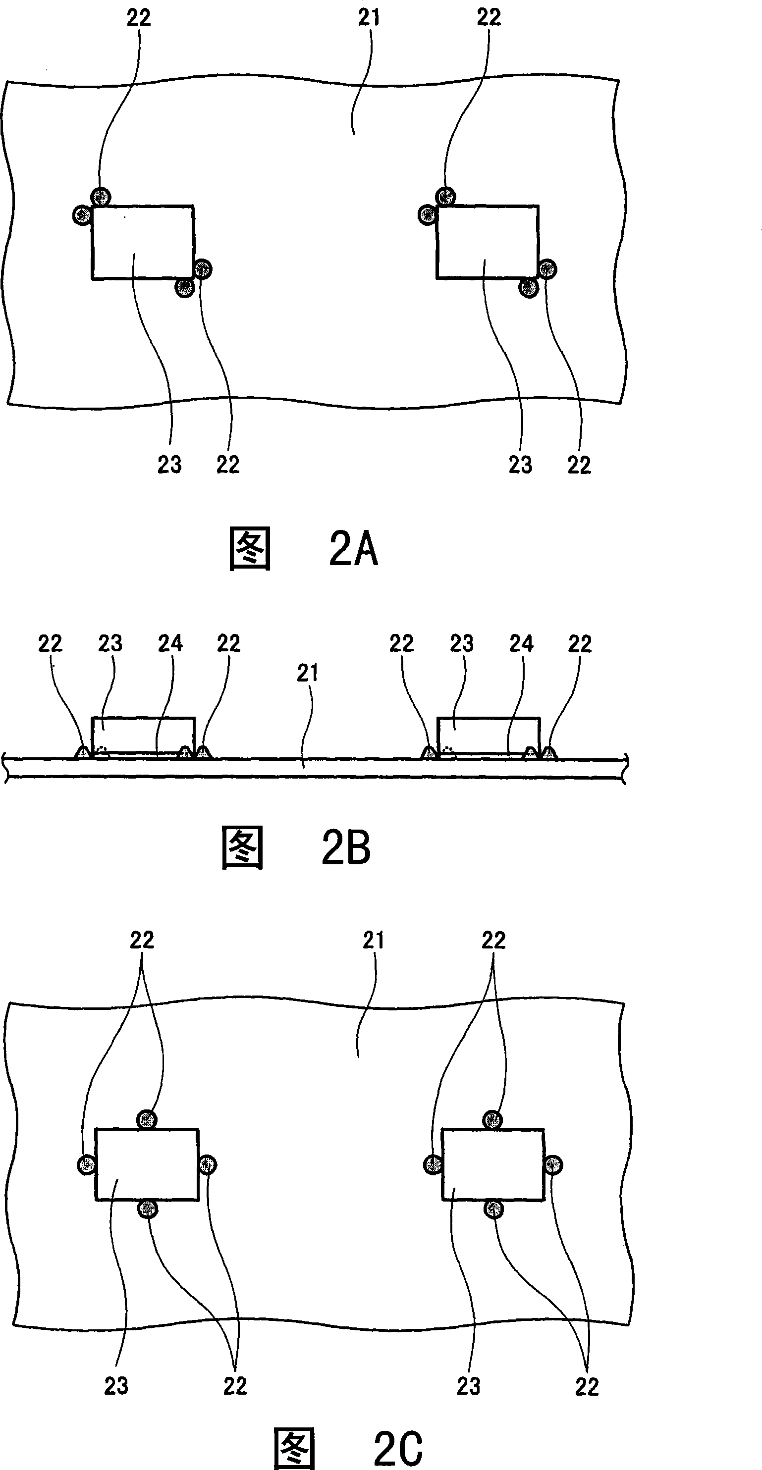
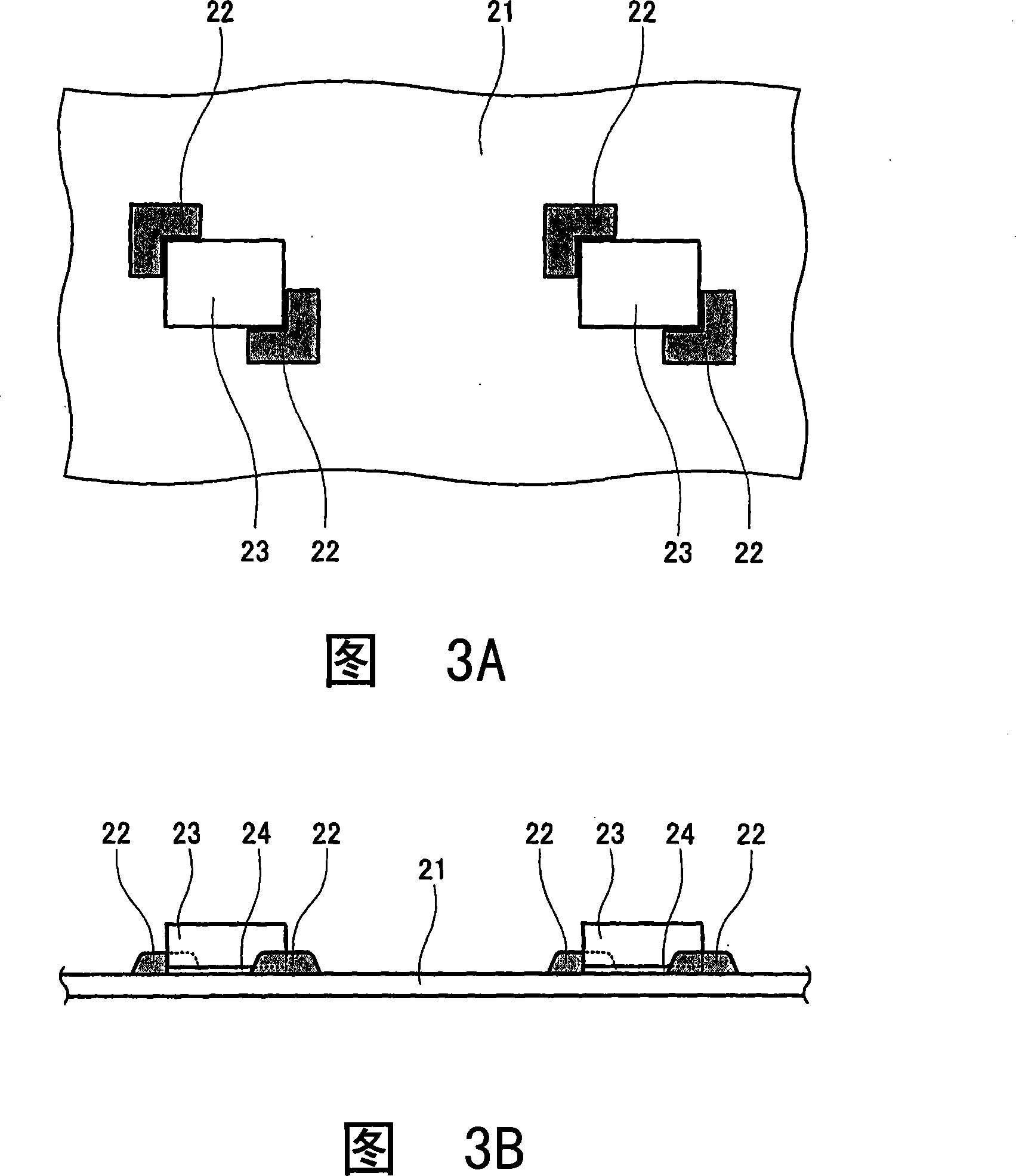
[0037] Hereinafter, a semiconductor device and a manufacturing method thereof according to an embodiment of the present invention will be described with reference to the drawings.

[0038] Here, a multi-chip module (resin-molded semiconductor device) is described as an example in which a plurality of semiconductor elements are arranged on the same surface, and one module is resin-sealed to realize multi-chip multi-chip.

[0039] Fig. 7 is a perspective view showing an example of the structure of a resin-molded semiconductor device according to an embodiment of the present invention. In the drawings, the sealing resin is not shown in order to show the structure of the resin-molded semiconductor device.

[0040] In FIG. 7 , 41 is a flat bare chip base (semiconductor element mounting portion) of the lead frame, 42 is a lead end of the lead frame, 43 is a suspension lead that is a part of the lead end, and 44 is a current that needs to flow to the bare chip base 41. 45 is a contr...


PUM


Abstract

The present invention discloses a semiconductor device and manufacture method thereof, variations in fastening positions of semiconductor elements are eliminated by forming protrusions on a die pad so as to enclose the semiconductor elements before an adhesive that fastens the semiconductor elements to the die pad is wetted and spread.

Description

technical field [0001] The present invention relates to a semiconductor device in which a plurality of semiconductor elements are arranged on the same surface and is intended to be multi-chip, and a method of manufacturing the same. Background technique [0002] In recent years, in order to realize the low cost and miniaturization of semiconductor devices, a multi-chip module in which a plurality of semiconductor elements with different functions are mounted on the same surface or a plurality of semiconductor elements formed by different processes has been proposed. . [0003] As a conventional multi-chip module, there is a structure in which a plurality of semiconductor elements are bonded to a flat die pad of a lead frame with an adhesive for bonding, and wirebonding is used to connect a plurality of semiconductor elements. Each semiconductor element is electrically connected to the inner lead part of the lead frame, and between the semiconductor elements. [0004] Howev...

Claims


Application Information

Patent Timeline
IPC IPC(8): H01L25/00H01L21/58
CPCH01L2224/26152H01L2924/01082H01L2924/01322
Inventor 藤原诚司
Owner PANASONIC CORP
Why Eureka
Try Eureka