Display panel

A technology of display panel and non-display area, applied in static indicators, instruments, etc., can solve the problems of low bonding success rate, affecting bonding success rate, shape expansion and shrinkage, etc., to achieve the effect of high bonding accuracy and improving yield

Active Publication Date: 2008-09-17
WUHAN CHINA STAR OPTOELECTRONICS TECH CO LTD
View PDF0 Cites 11 Cited by
  • Summary
  • Abstract
  • Description
  • Claims
  • Application Information

AI Technical Summary

Problems solved by technology

[0005] However, due to the material properties of the pins 122, 132, when the pins 132 of the driver chip are bonded with the pins 122 in the pad area 120 by thermocompression, the pins 122 will follow it in the pad area 120. The configuration positions are different, but there are problems of unstable quality such as shape expansion and contraction, position offset, etc.
These problems will affect the bonding success rate between the pins 132 of the driver chip 130 and the pins 122 in the pad area 120
When the bonding success rate between the pins 132 of the driver chip 130 and the pins 122 on the substrate 110 is low, the display quality of the display panel 100 will be seriously affected.

Method used


Image

  • Display panel
  • Display panel
  • Display panel

Examples


no. 1 example

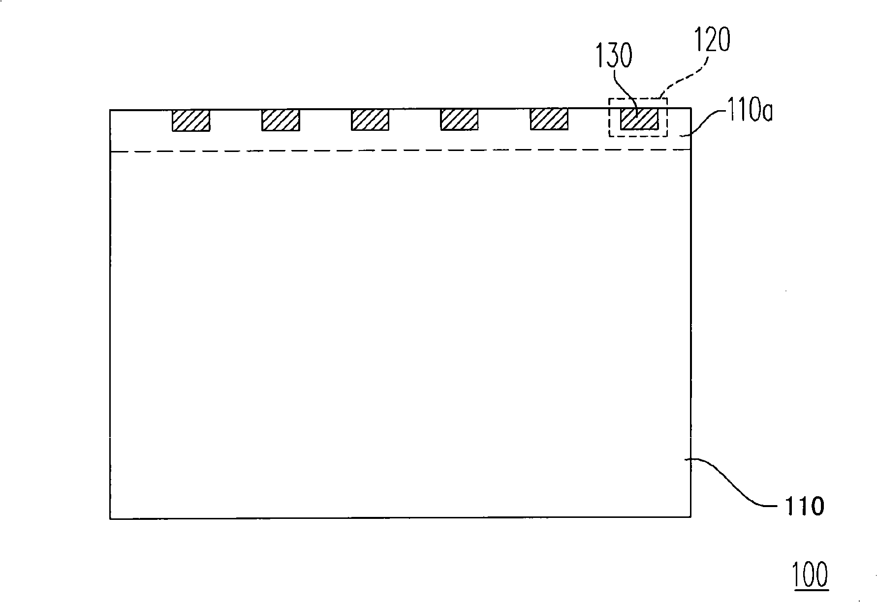
[0049] Figure 2A is a schematic diagram of the display panel of the first embodiment of the present invention, and Figure 2B for Figure 2A A partial enlarged view of the substrate of the display panel. Please also refer to Figure 2A and 2B , the display panel 2000 of this embodiment includes a substrate 2100 and a plurality of driving chips 2200 . The substrate 2100 of this embodiment is an active device array substrate, and the substrate 2100 has a display area 2120 and a non-display area 2140 , wherein the non-display area 2140 surrounds the display area 2120 . The pad area 2142 is located in the non-display area 2140, and the pad area 2142 has a central line 2142a. In addition, a plurality of first pins 2144 with the same length are arranged in each pad area 2142 , and these first pins 2144 are symmetrically arranged in parallel in the pad area 2142 with the center line 2142 a as the center.

[0050] It is worth noting that, in each pad area 2142 of the display pa...

no. 2 example

[0067] This embodiment is substantially the same as the first embodiment, and the reference numerals of elements similar to those of the first embodiment represent the same or similar elements, and will not be repeated here. Differences between this embodiment and the first embodiment will be described below.

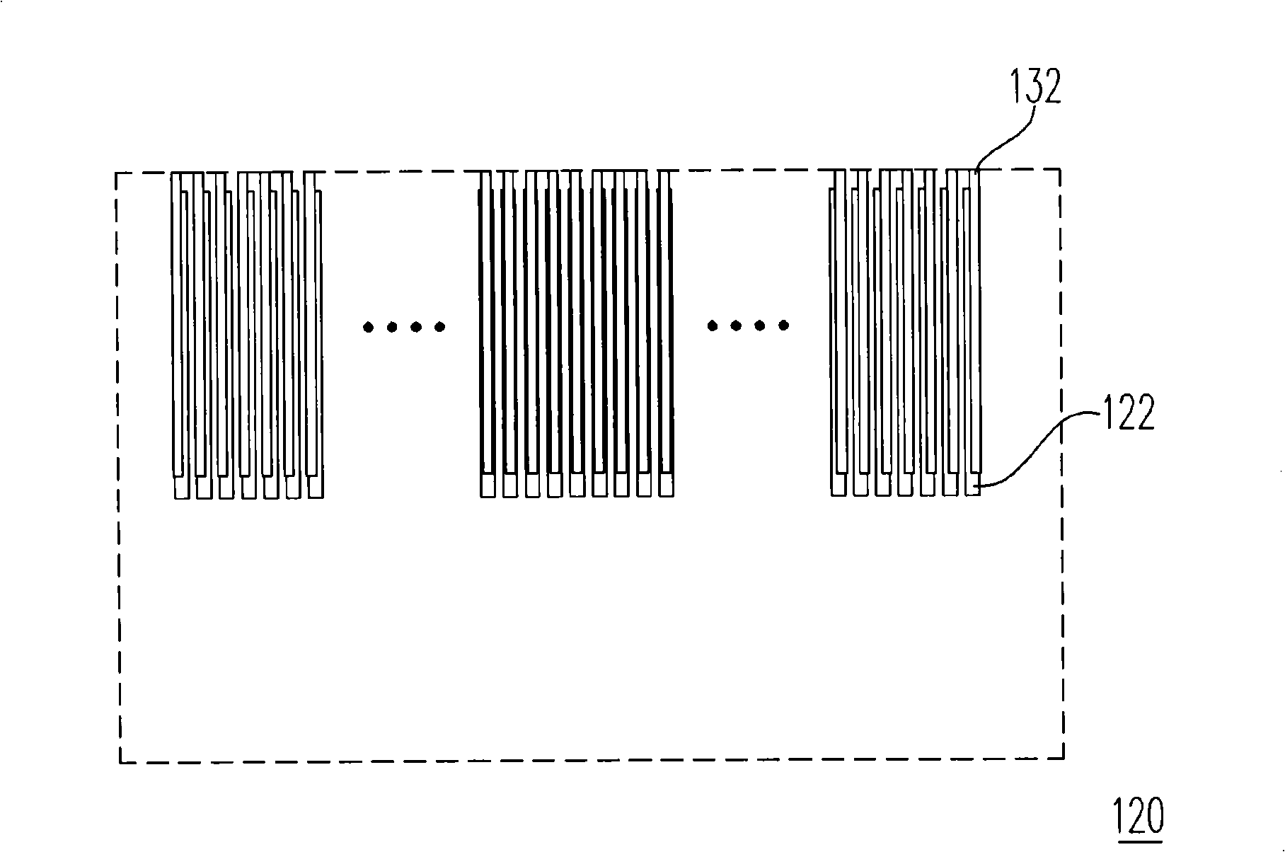
[0068] image 3 It is a schematic diagram of bonding the first pins of the substrate to the second pins of the driving chip in the display panel according to the second embodiment of the present invention. Please refer to image 3 , the difference between this embodiment and the first embodiment is that: in each pad area 3142 of the display panel (not marked) in this embodiment, the width of the first pin 3144 will increase as it is in the pad area 3142 The location of the configuration within varies. In detail, the first pins 3144 are disposed from the center line 3142 a of the pad area 3142 to the outside, and the width of the first pins 3144 may gradually become w...

no. 3 example

[0072] This embodiment is substantially the same as the first and second embodiments, and similar reference numerals represent the same or similar components, and will not be repeated here. Figure 4 It is a schematic diagram of bonding the first pins of the substrate to the second pins of the driving chip in the display panel according to the third embodiment of the present invention. Please refer to Figure 4 The difference between this embodiment and the first and second embodiments lies in: in each pad area 4142 of the display panel (not marked) of this embodiment, the distance between two adjacent first pins 4144, and The width of each first pin 4144 varies according to its position in the pad area 4142 . In detail, the first pins 4144 are arranged outside the center line 4142a of the pad area 4142, the width of the first pins 4144 gradually increases, and the distance between two adjacent first pins 4144 gradually widens. .

[0073] In this way, the traditional proble...


PUM


Abstract

The invention discloses a display panel, comprising a substrate and a plurality of drive chips. The substrate has a plurality of pad areas located in a non-display area of the substrate; each pad area is configured with a polarity of first pins with the same length; at least one of the space between two adjacent first pins and the width of each first pin varies along with the configuration position. The drive chips are configured in the non-display area of the substrate; each drive chip has a plurality of second pins which are respectively connected to the first pins.

Description

technical field [0001] The present invention relates to a display panel, and in particular to a display panel in which the pins of a chip can be accurately bonded to the pins of a substrate. Background technique [0002] Cathode ray tube (CRT) displays have been monopolizing the display market due to their excellent display quality and economy. However, cathode ray tube displays have radiation and are bulky and take up space. In recent years, thanks to the rapid progress of semiconductor components, flat panel displays with high image quality, good space utilization efficiency, low power consumption, and no radiation have gradually become the mainstream of the market. [0003] The components of the flat panel display include a display panel, a light source for providing sufficient brightness for the display panel, and a driver chip disposed on the substrate of the display panel, wherein the driver chip is used to drive circuits inside the display panel so that the display p...

Claims


Application Information

Patent Timeline
IPC IPC(8): G09G3/28G09G3/30G09G3/36
Inventor 陈永坚
Owner WUHAN CHINA STAR OPTOELECTRONICS TECH CO LTD
Why Eureka
Try Eureka