Copper surface chemical mechanical polishing/planarization method

A chemical-mechanical, copper-surface technology, applied in electrical components, semiconductor/solid-state device manufacturing, circuits, etc., can solve problems such as increasing process complexity, increasing manufacturing costs, and achieving the effect of flattening

Inactive Publication Date: 2008-10-29
SEMICON MFG INT (SHANGHAI) CORP
View PDF1 Cites 2 Cited by
  • Summary
  • Abstract
  • Description
  • Claims
  • Application Information

AI Technical Summary

Problems solved by technology

However, this method has higher requirements on the grinding liquid, and it is undoubtedly necessary to add reactive reagents such as potassium iodate, hydrogen peroxide, ferric nitrate, or ammonium persulfate. Increased manufacturing costs and increased process complexity

Method used


Image

  • Copper surface chemical mechanical polishing/planarization method
  • Copper surface chemical mechanical polishing/planarization method
  • Copper surface chemical mechanical polishing/planarization method

Examples


Embodiment Construction

[0031] In order to make the above objects, features and advantages of the present invention more comprehensible, specific implementations of the present invention will be described in detail below in conjunction with the accompanying drawings.

[0032] In the following description, numerous specific details are set forth in order to provide a thorough understanding of the present invention. However, the present invention can be implemented in many ways other than those described here, and those skilled in the art can make similar extensions without departing from the connotation of the present invention. Accordingly, the invention is not limited to the specific implementations disclosed below.

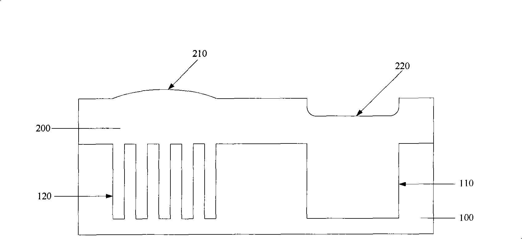
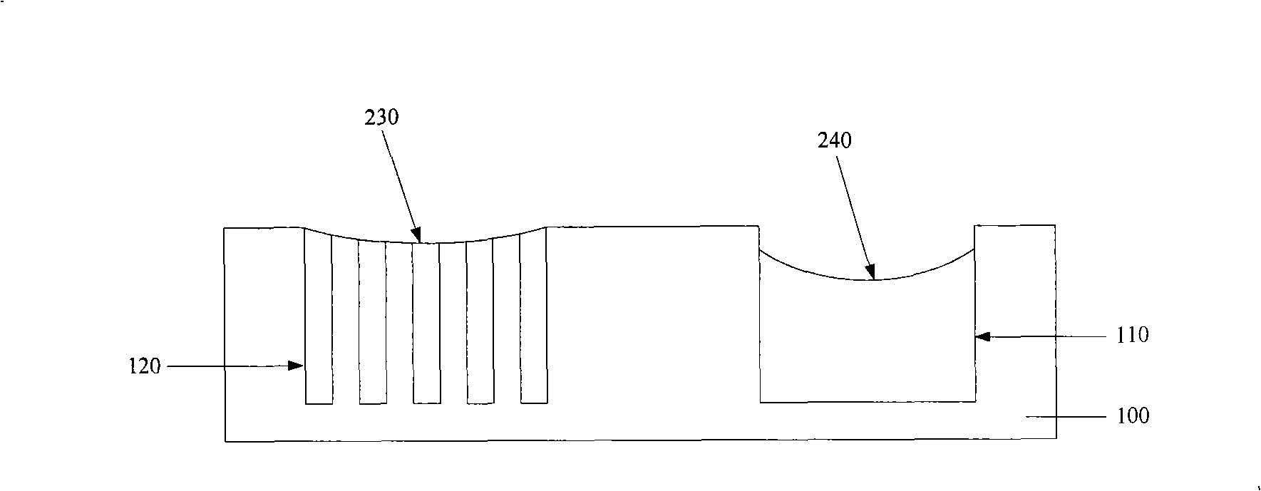
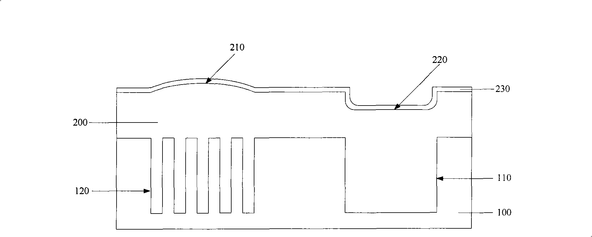
[0033] Figure 3 to Figure 6 A schematic cross-sectional view of a device illustrating a preferred embodiment of the present invention. The schematic diagrams described are only examples, which should not limit the scope of protection of the invention here. first as image 3 As sho...


PUM


Abstract

The invention discloses a rubbing planarization method for a chemical machine with a copper surface, which includes: the step of depositing a medium layer on the copper surface and the step of carrying out rubbing on the copper surface with the medium layer. The rubbing planarization method for the chemical machine with a copper surface of the invention can realize the planarization of the copper surface and the medium layer surface and avoid a dishing phenomenon from from being generated.

Description

technical field [0001] The invention relates to the technical field of semiconductor manufacturing, in particular to a method for chemical mechanical polishing and planarization of copper surfaces. Background technique [0002] With the rapid development of semiconductor manufacturing technology, the line width feature size of semiconductor devices has entered the deep submicron structure. In order to increase the computing speed of the chip, it is necessary to effectively reduce the time delay caused by the impedance. Therefore, low dielectric constant materials are mostly used in semiconductor devices, and metal copper is widely used as an interconnect structure to reduce the resistance of metal wires. The interconnection structure is usually formed by a damascene method, that is, through holes are etched in one or more dielectric layers on the substrate, and then metal is deposited in the through holes. Although the impedance of copper is lower than that of aluminum or ...

Claims


Application Information

Patent Timeline
Patent Type & Authority Applications(China)
IPC IPC(8): H01L21/321H01L21/768
CPCH01L21/3212H01L21/31116
Inventor 朱旋蔡孟峰
Owner SEMICON MFG INT (SHANGHAI) CORP
Why Eureka
Try Eureka