Chip packaging outer lead wire molding die

A technology for installing external leads and forming molds, which is applied in the manufacture of electrical components, electrical solid devices, semiconductor/solid devices, etc., can solve the problems of easily damaged packaging blocks, etc., and achieve the effect of good coplanarity and good electrical connection characteristics

Inactive Publication Date: 2008-11-26
SEMICON MFG INT (SHANGHAI) CORP
View PDF1 Cites 2 Cited by
  • Summary
  • Abstract
  • Description
  • Claims
  • Application Information

AI Technical Summary

Problems solved by technology

However, when using the pressing block for forming the outer lead to form the outer lead of the TSOP package block, it is easy to damage the package block, causing it to break and be damaged.

Method used


Image

  • Chip packaging outer lead wire molding die
  • Chip packaging outer lead wire molding die
  • Chip packaging outer lead wire molding die

Examples


Embodiment Construction

[0033] The specific embodiments of the present invention will be described in detail below in conjunction with the accompanying drawings.

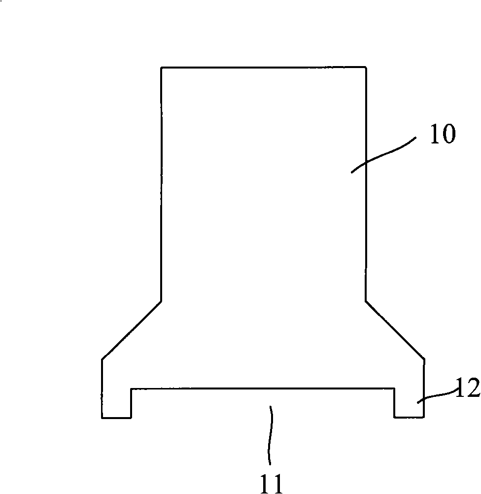
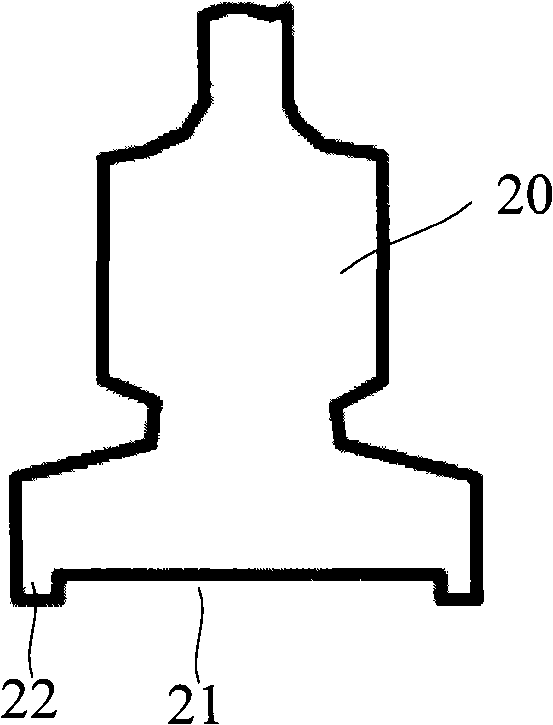
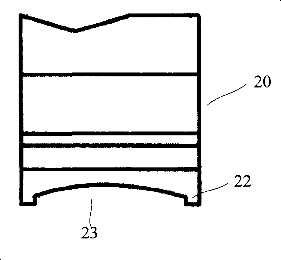
[0034] In order to achieve thin packaging, lead-on-chip packaging structure is adopted in the TSOP packaging process. After the chip is plastic-encapsulated, the thickness of the resin on the top and bottom of the chip is different, resulting in different shrinkage of the resin on the top and bottom of the chip during the cooling process after plastic packaging, resulting in the formation of TSOP packaging blocks. produce warping. This warpage leads to poor coplanarity of the outer leads when the outer leads are formed through the molding die and the stamping head after the chip is plastic-packed, which in turn causes the outer leads to be in contact with the PCB or other substrates when the TSOP package block is mounted. The solder joints on other substrates are not in good contact, or even open circuit, which may easily cause electrical ...


PUM

PropertyMeasurementUnit
depthaaaaaaaaaa
depthaaaaaaaaaa
thicknessaaaaaaaaaa

Abstract

A chip package outer lead mould is used for molding a small size thin packaging block outer lead which is equipped with warpage, and comprises a fundamental portion. The fundamental portion is equipped with an outer lead pressing portion which is provided with a contact portion contact with the small size thin packaging block outer lead, wherein a groove engaged with the small size thin packaging block is formed between the outer lead pressing portion. The depth of the groove is equal to the maximum distance between the outer lead and the surface of the small size thin packaging block engaged with the groove, and the depth of the groove is the minimum distance between the position of the small size thin packaging block engaged with the groove and the contact portion of the outer lead pressing portion. The chip package outer lead mould can enable the flatness of a molded outer lead to be better and avoid damaging the packaging block in molding process.

Description

technical field [0001] The invention relates to the technical field of semiconductor packaging, in particular to a thin small outline package (Thin Small Outline Package, TSOP) outer lead molding die for a chip. Background technique [0002] The TSOP package is a technology in which pins are made around the chip, and the packaged chip pins are directly soldered to the surface of the printed circuit board (PCB) by using Surface Mounting Technology (SMT). TSOP packaging has the advantages of high yield and low price, so it has been widely used. In the TSOP packaging process, in order to achieve thin and small size packaging, the lead on chip packaging (Lead OnChip, LOC) structure is generally used in the plastic packaging process, resulting in different thicknesses of the plastic packaging resin on the top and bottom of the chip after the chip is plastic packaged, resulting in cooling after plastic packaging. During the process, the shrinkage of the resin on the top and botto...

Claims


Application Information

Patent Timeline
Patent Type & Authority Applications(China)
IPC IPC(8): H01L21/00H01L21/60B21F1/00H05K13/00H05K13/04
CPCH01L2924/0002H01L21/4842H01L2924/00
Inventor 舒海波唐智能蒲光荣李敏
Owner SEMICON MFG INT (SHANGHAI) CORP
Why Eureka
Try Eureka