Electronic device carrier adapted for transmitting high frequency signals

a high-frequency signal and electronic device technology, applied in the direction of cross-talk/noise/interference reduction, printed circuit aspects, printed circuit non-printed electric components association, etc., can solve the problem of difficult to understand if a switching transition actually took place, affecting the performance of the electronic system as a whole, and affecting the coplanarity of pads

Inactive Publication Date: 2006-03-21
IBM CORP
View PDF5 Cites 11 Cited by
  • Summary
  • Abstract
  • Description
  • Claims
  • Application Information

AI Technical Summary

Benefits of technology

[0013]It is still another object of the invention to provide an electronic device carrier adapted for transmitting high frequency signals that improve pads coplanarity so as to provide reliable contacts between pads and electronic device I / O.
[0014]It is a further object of the invention to provide an electronic device carrier adapted for transmitting high frequency signals that provide reliable adhesion between its different dielectric material layers.

Problems solved by technology

When the chip works at a high frequency, e.g. more than 1 GHz, the influence of the electronic device carrier may severely affects the performance of the electronic system as a whole.
As a consequence, the integrity of the electromagnetic wave propagated along the transmission line is not preserved.
The above described discontinuities in the transmission line reduce the opening of the eye diagram; therefore, it is quite difficult to understand if a switching transition has actually taken place or if the shift of a signal baseline is due to a background noise.
These drawbacks are particular acute in modern electronic systems working with a reduced level of a power supply voltage (down to 1.2 V).

Method used


Image

  • Electronic device carrier adapted for transmitting high frequency signals
  • Electronic device carrier adapted for transmitting high frequency signals
  • Electronic device carrier adapted for transmitting high frequency signals

Examples


Embodiment Construction

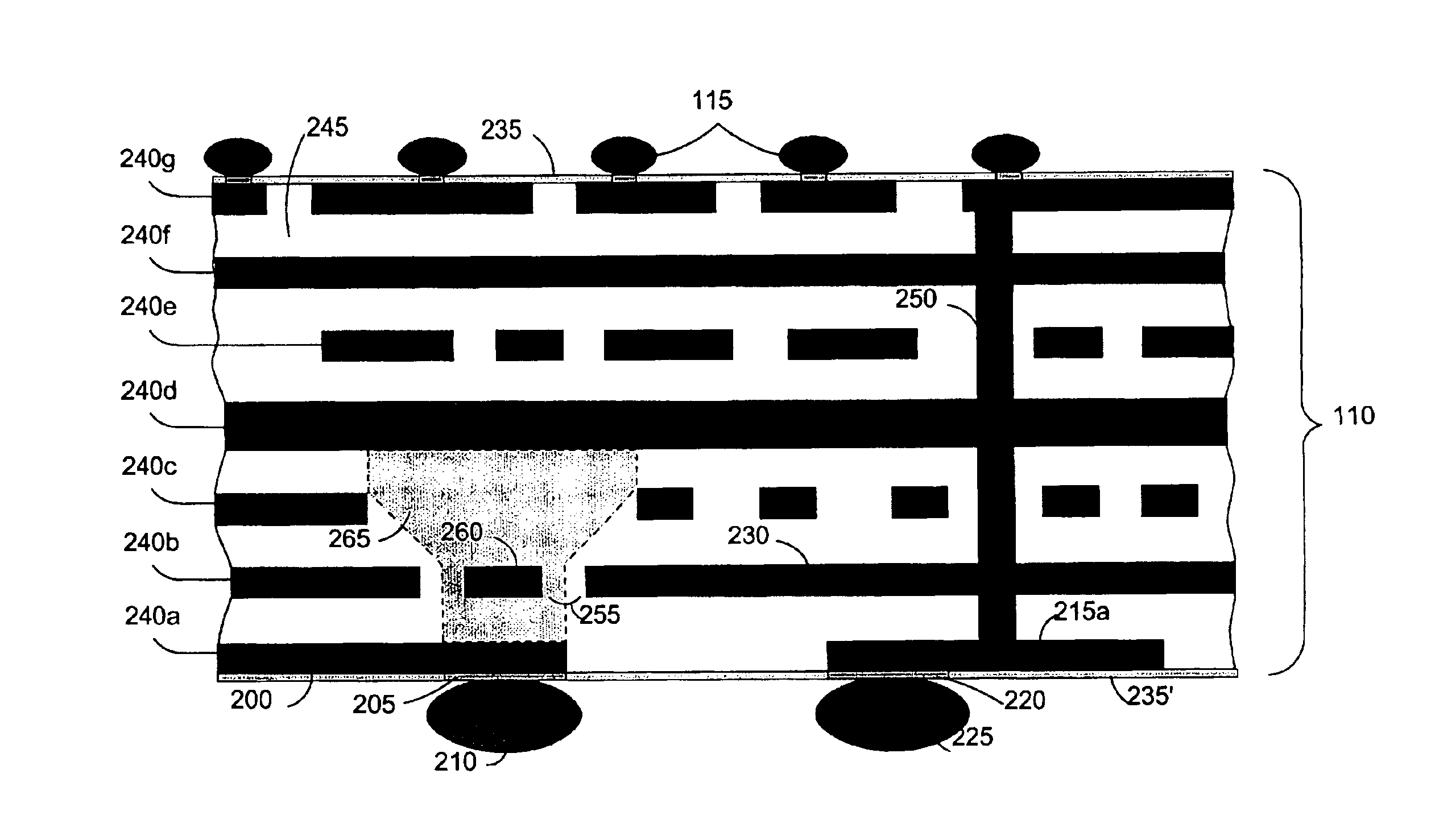
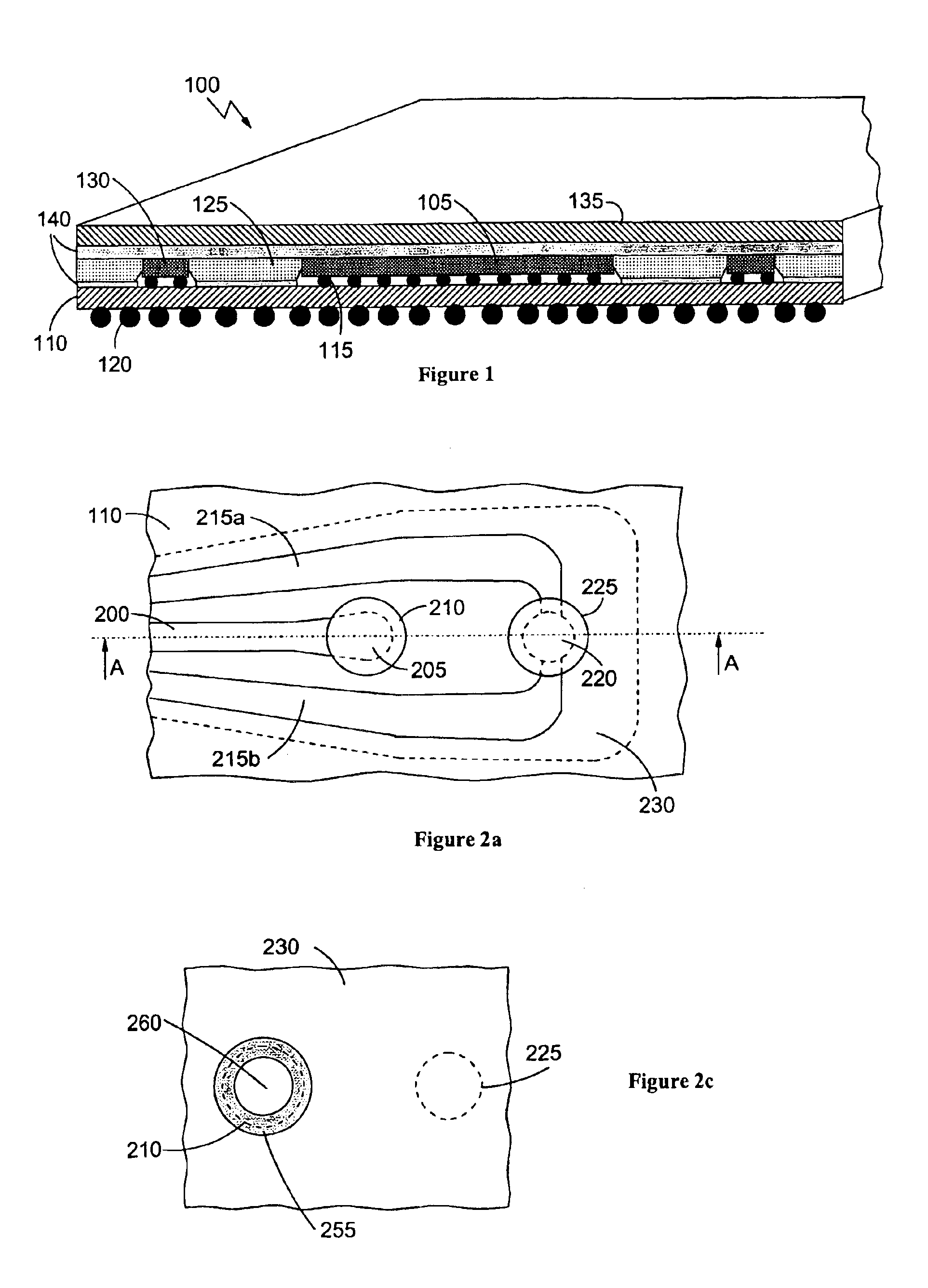
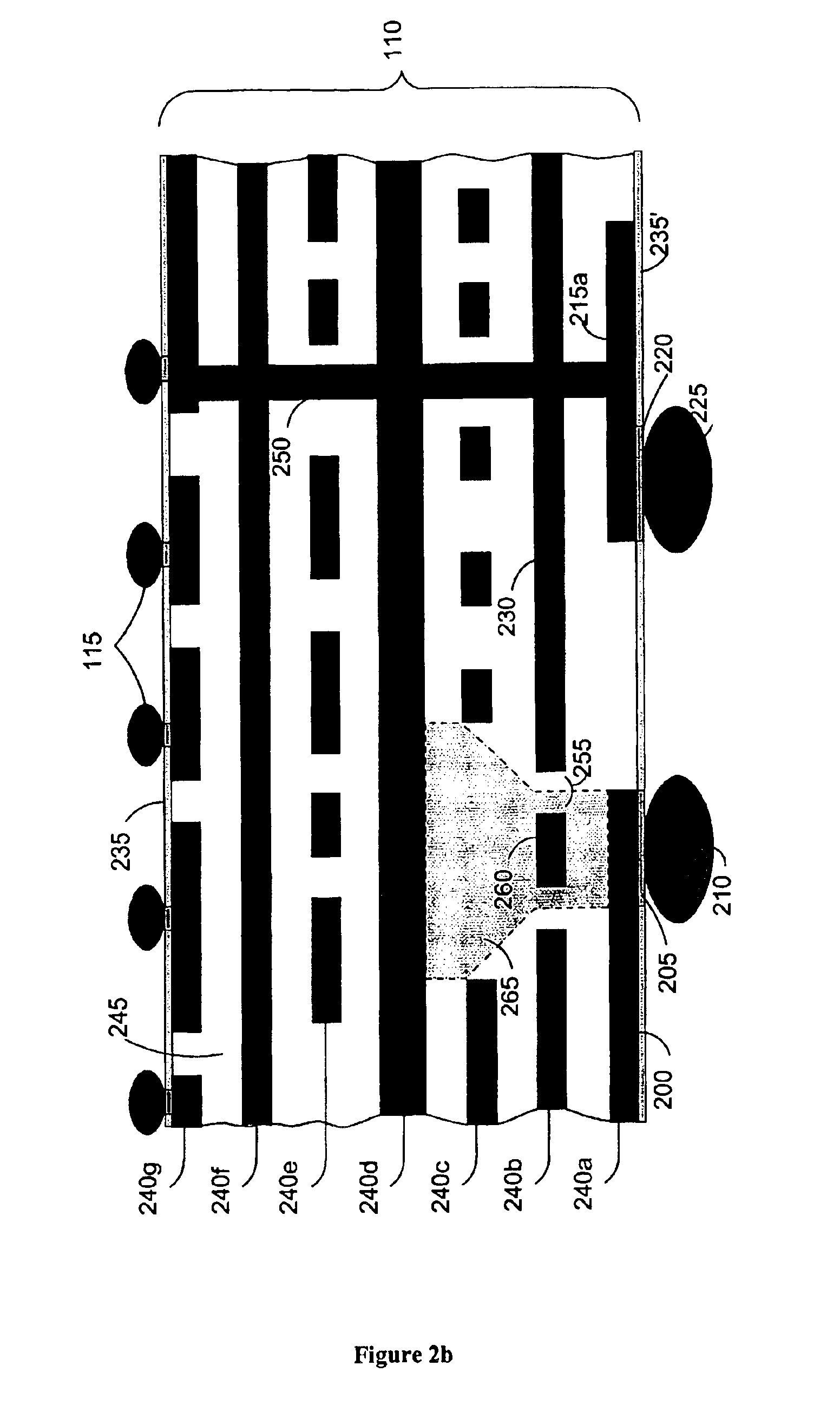
[0023]For sake of illustration, the following description is based on Ball Grid Array (BGA) package wherein chip to chip carrier interconnection is performed with Controlled Collapse Chip Connection (IBM C4 technology), widely known as Flip-Chip Attach (FCA). Such technology provides high I / O density, uniform chip power distribution, high cooling capability and high reliability.

[0024]With reference in particular to FIG. 1, there is depicted an electronic module 100 of the BGA type. The electronic module 100 includes a chip 105 of semiconductor material, wherein a power circuit working at a high frequency, e.g. with a clock rate of 5 GHz, is integrated. Chip 105, supplied by a low voltage power supply, e.g. 1.2V., is mounted on a laminate chip carrier 110 comprising several conductive layers, e.g. made of copper, insulated from each other by means of a dielectric material, e.g. Polytetraflouroethylene (PTFE). Chip 105 to chip carrier 110 interconnection is performed with C4 balls 115...


PUM


Abstract

An electronic device carrier (110) adapted for transmitting high-frequency signals, including a circuitized substrate with a plurality of conductive layers (240a to 240g) insulated from each other, the conductive layers being arranged in a sequence from a first one of the conductive layers (240a) wherein a plurality of signal tracks (200) each one ending with a contact area (205) for transmitting a high-frequency signal are formed, and a reference structure (215a, 215b, 230) connectable to a reference voltage or ground for shielding the signal tracks the reference structure includes at least one reference track (230) formed in a second one of the conductive layers (240b) adjacent to the first conductive layer and at least one further reference track formed in one of the conductive layers (240d) different from the first and second conductive layer, a portion of each signal track excluding at least the area corresponding to the orthographic projection of associated contact area being superimposed in plan view to a corresponding reference track and at least a part of the area corresponding to the orthographic projection of the contact area associated to each signal track being superimposed in plan view to a corresponding further reference track with interposition of a floating conductive track, i.e. a track not connected to any signal, reference voltage or ground track.

Description

FIELD OF THE INVENTION[0001]The present invention relates to the field of electronic device interconnection and more specifically to an electronic device carrier adapted for transmitting high frequency signals.BACKGROUND OF THE INVENTION[0002]Several types of electronic components are implemented with a circuit, which is integrated in a chip of semiconductor material. The chip is typically mounted on a carrier, so as to protect the chip from mechanical stresses, and is then encapsulated in a package. The chip carrier includes an insulating substrate with conductive tracks; each track is bonded to a corresponding terminal of the chip, and ends with a contact pad, typically for connection to a printed circuit board. Likewise, printed circuit board generally comprises several conductive layers formed in an insulating material, adapted to transmit signals between several electronic devices or between electronic devices and connectors.[0003]When switching speeds of devices goes above 1 G...

Claims


Application Information

Patent Timeline
Patent Type & Authority Patents(United States)
IPC IPC(8): H01L23/48H01L23/12H01L23/16H01L23/36H01L23/498H01L23/66H01L25/065H05K1/02H05K1/11
CPCH01L23/16H01L23/49822H01L23/66H01L25/0655H05K1/0219H01L23/36H01L2224/16225H01L2223/6616H01L2223/6627H01L2224/73253H01L2924/01057H01L2924/15153H01L2924/1517H01L2924/15173H01L2924/15311H01L2924/16195H01L2924/1903H01L2924/3011H01L2924/3025H05K1/111H05K2201/09236H05K2201/09781H01L2224/16227H01L2224/73204H05K1/18H01L23/498H05K1/02
Inventor ALCOE, DAVIDNOWAK, RONALDPREDA, FRANCESCOOGGIONI, STEFANO SERGIO
Owner IBM CORP
Why Eureka
Try Eureka