Luminous diode encapsulation method with high efficiency light emitting effect and its packaging structure
A technology of light-emitting diodes and luminous effects, which is applied in the manufacture of electrical components, electrical solid devices, semiconductor/solid-state devices, etc., which can solve problems such as inconvenience, poor light efficiency and loss of light rods, and achieve the effect of shortening the process time
- Summary
- Abstract
- Description
- Claims
- Application Information
AI Technical Summary
Problems solved by technology
Method used
Image

Examples
Embodiment Construction
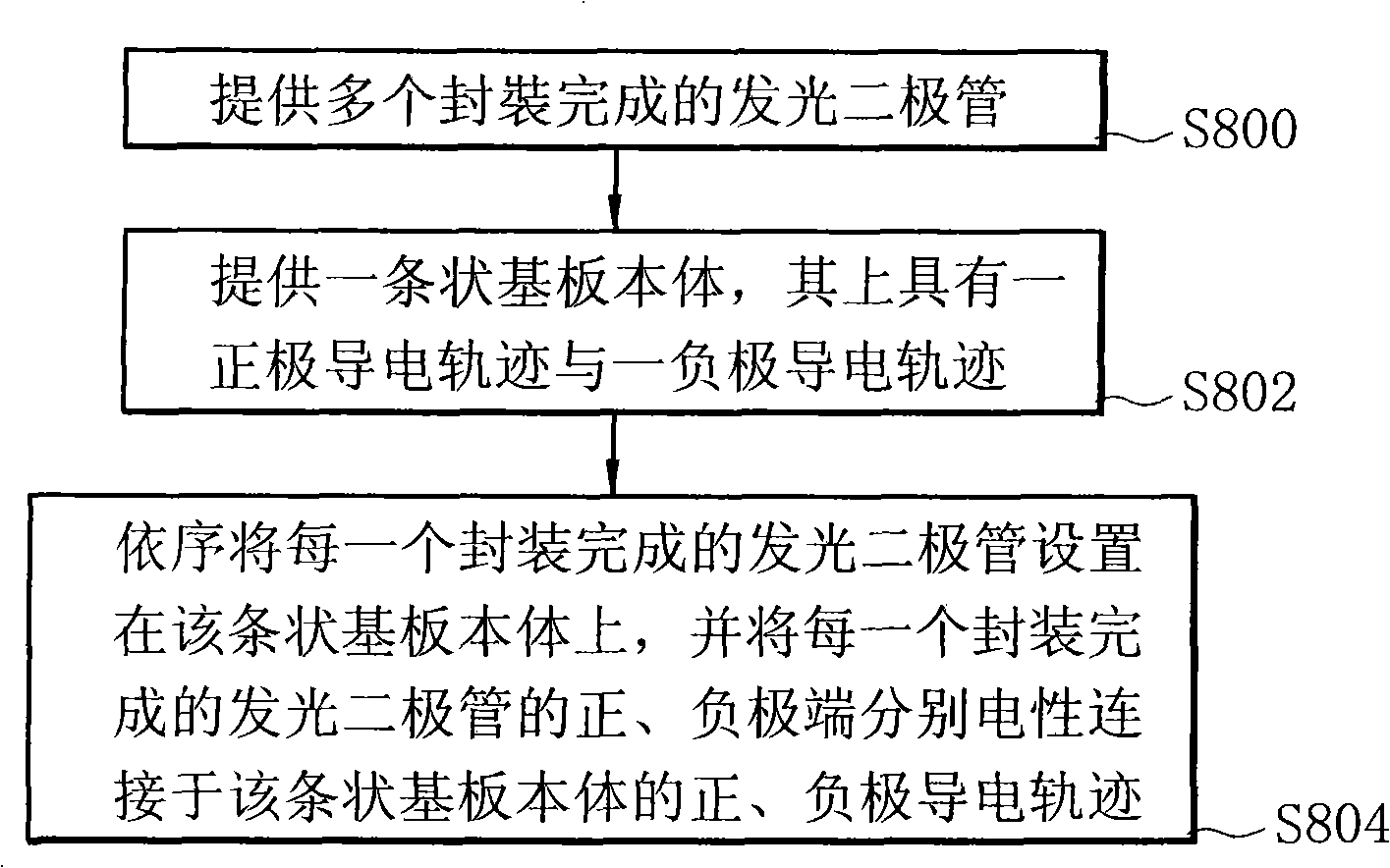
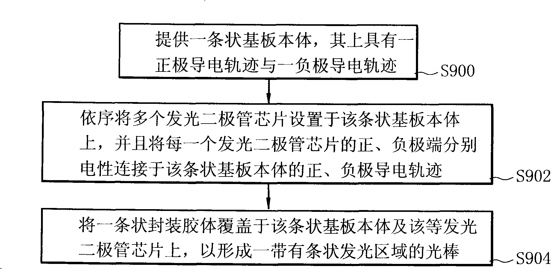
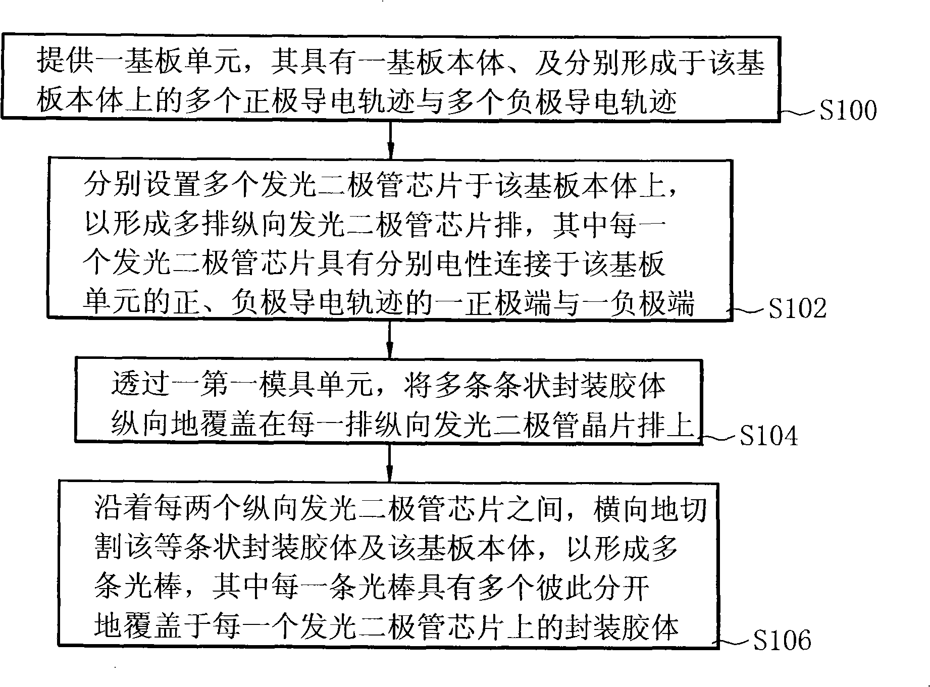
[0063] see image 3 , image 3 a to image 3 d, and image 3 A to image 3 D shows. image 3 It is a flow chart of the first embodiment of the packaging method of the present invention, image 3 a to image 3 d is a schematic diagram of the packaging process of the first embodiment of the packaging structure of the present invention, image 3 A to image 3 D is a schematic cross-sectional view of the packaging process of the first embodiment of the packaging structure of the present invention, respectively. Depend on image 3 It can be seen from the flow chart that the first embodiment of the present invention provides a method for packaging light-emitting diodes with high-efficiency light-emitting effects, which includes the following steps:
[0064] First of all, please cooperate image 3 a and image 3 As shown in A, a substrate unit (substrate unit) 1 is provided, which has a substrate body (substrate body) 10, and a plurality of positive electrode traces (posit...
PUM
 Abstract
Description
Claims
Application Information
 - Generate Ideas
- Intellectual Property
- Life Sciences
- Materials
- Tech Scout
- Unparalleled Data Quality
- Higher Quality Content
- 60% Fewer Hallucinations
Browse by: Latest US Patents, China's latest patents, Technical Efficacy Thesaurus, Application Domain, Technology Topic, Popular Technical Reports.
© 2025 PatSnap. All rights reserved.Legal|Privacy policy|Modern Slavery Act Transparency Statement|Sitemap|About US| Contact US: help@patsnap.com