Fuse-wires structure and forming method thereof

A fuse structure and fuse technology, which are applied in the manufacturing of electrical components, electric solid-state devices, semiconductor/solid-state devices, etc., can solve the problems of increasing process costs, increasing masks, and incompatibility, and achieving the effect of increasing process costs.

Active Publication Date: 2008-11-26
SEMICON MFG INT (SHANGHAI) CORP +1
View PDF1 Cites 5 Cited by
  • Summary
  • Abstract
  • Description
  • Claims
  • Application Information

AI Technical Summary

Problems solved by technology

However, the above-mentioned process is not compatible with the existing standard CMOS process. At the same time, in the manufacturing process, additional masks and doping processes are required, which increases the process cost.

Method used


Image

  • Fuse-wires structure and forming method thereof
  • Fuse-wires structure and forming method thereof
  • Fuse-wires structure and forming method thereof

Examples


no. 1 example

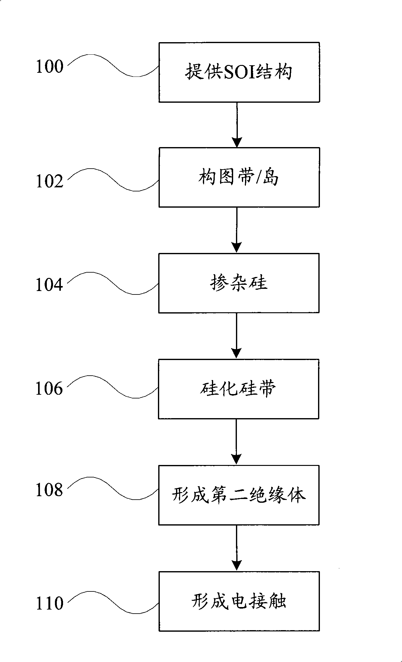
[0028] The present invention first provides a first embodiment of a method for forming a fuse, including: providing a semiconductor substrate; sequentially forming a first dielectric layer and a polysilicon layer on the semiconductor substrate, and the polysilicon layer adopts a polysilicon layer forming a transistor ; Forming at least two doped regions in the polysilicon layer, the conductivity types of the two adjacent doped regions are opposite; forming a silicide layer on the polysilicon layer with at least two doped regions; forming a silicide layer on the silicide layer second dielectric layer; form a via hole in the second dielectric layer, the via hole exposes the silicide layer; fill the via hole with a conductive material and be in contact with the silicide layer; fill the conductive material on the second dielectric layer The via locations of the material form the metal pads.

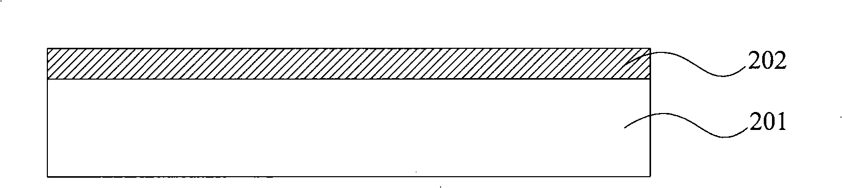
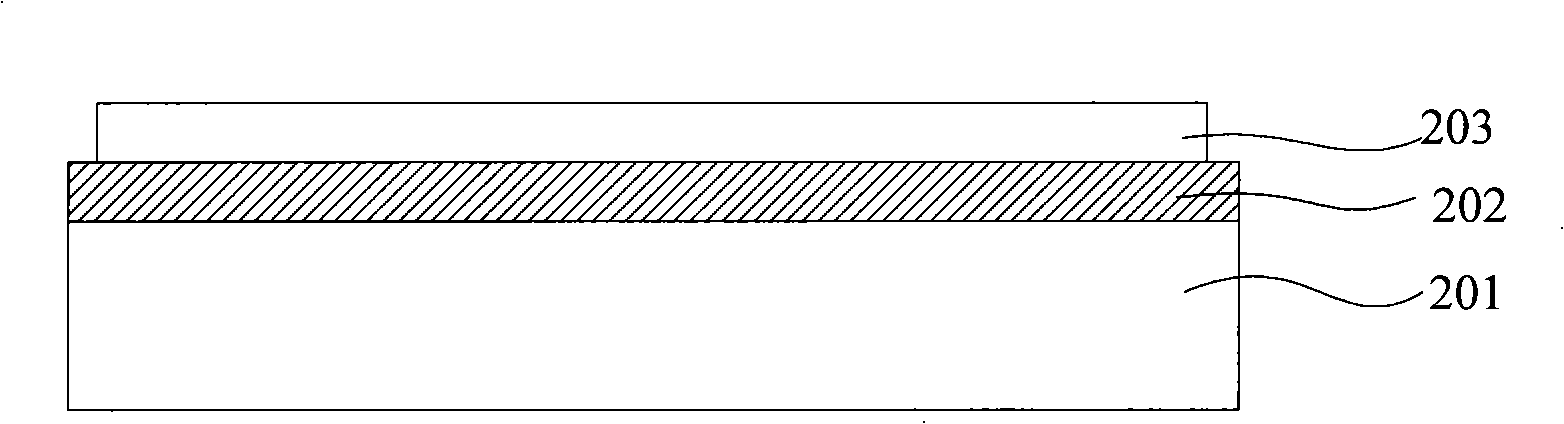
[0029] First refer to figure 2 , providing a semiconductor substrate 201, the semicondu...


PUM


Abstract

A fuse forming method includes sequentially forming a first medium layer and a polysilicon layer, forming at least two adjacent doped areas with opposite conduction types, sequentially forming a silicide layer and a second medium layer, forming a through hole filled with conductive material on the second medium layer, and forming a metal gasket on the through hole. The invention accordingly provides a fuse structure, which forms different doped areas of the fuse structure by utilizing the polysilicon layer which forms a transistor as the polysilicon layer of the fuse structure, and using source /drain ion implantation and ion implantation forming a source /drain extending area. Before and after programming, the fuse structure has large resistance difference, which is favorable for status detection before and after programming, and simultaneously completely compatible with the existing standard CMOS technology, does not increase extra masks and doping process and technological cost.

Description

technical field [0001] The invention relates to the technical field of semiconductors, in particular to a fuse structure and a forming method thereof. Background technique [0002] With the miniaturization and increasing complexity of semiconductor technology, semiconductor components are more susceptible to various defects or impurities, and the failure of a single wire, diode or transistor often constitutes a defect of the entire chip. Therefore, in order to solve this problem, some fuses are formed in the integrated circuit in the prior art to ensure the availability of the integrated circuit. [0003] In general, fuses are used to connect redundant circuits in integrated circuits. Once the circuits are found to be defective, these redundant circuits can be used to repair or replace the defective circuits. Taking the memory structure as an example, the existing technology will make some fuse structures on the top layer of the structure. Wire jumpers are used to replace ...

Claims


Application Information

Patent Timeline
Patent Type & Authority Applications(China)
IPC IPC(8): H01L21/768H01L23/525
Inventor 欧阳雄罗文哲李智黄强姜敏
Owner SEMICON MFG INT (SHANGHAI) CORP
Why Eureka
Try Eureka