Regulation test system and method of on-chip system as well as on-chip system
A system-on-chip and commissioning technology, applied in the field of system-on-chip, can solve problems such as inability to perform commissioning
- Summary
- Abstract
- Description
- Claims
- Application Information
AI Technical Summary
Problems solved by technology
Method used
Image

Examples
Embodiment 1
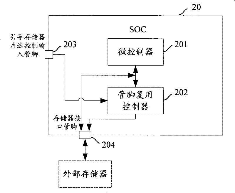
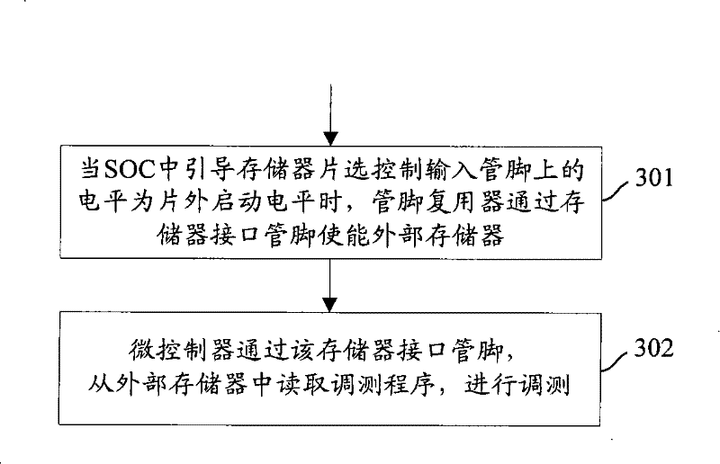
[0097] The external boot memory in this embodiment is NOR flash memory, and the memory interface pins may include read and write data pins and digital logic function pins. Among them, the read and write data pins are a collection of pins with any one or more functions of read function, write function, and data transmission function, and are used as the transmission channel for the commissioning program from the external boot memory to the inside of the system on chip; digital logic Function pins are a collection of pins such as address pins and chip select pins, which are used for the pin multiplexing controller to enable the external boot memory through the digital logic function pins.
[0098] Figure 4 A schematic structural diagram of the commissioning system in this embodiment is shown. see Figure 4 , the commissioning system includes: SOC 40 and non-flash memory 41 as an external boot memory; Select control input pin 404, read / write data pin 405 and digital logic fun...
Embodiment 2
[0118] This embodiment considers that each part of the SOC needs to be verified during the commissioning phase. Therefore, a static random access memory is added inside the SOC to store the commissioning program read from the external boot memory, so as to release the read and write data pins. And the occupancy of the digital logic function pins is convenient for debugging these two pins.
[0119] Image 6 A schematic structural diagram of the commissioning system in this embodiment is shown. see Image 6 , the commissioning system includes: SOC 60 and NOR flash memory 61 as an external boot memory; and, the SOC60 in the figure is in Figure 4 SRAM 607 is added on the basis of .
[0120] The microcontroller 601 in this embodiment is similar to the microcontroller 401 in Embodiment 1, the difference is that the microcontroller 601 in this embodiment also allocates and or non-flash memory for the SRAM 607 through the memory controller different addresses, and obtain the debu...
Embodiment 3
[0143] In this embodiment, adopt such as safe digital storage (SD, Secure Digital Memory) card, NAND flash memory, memory stick (MS, Memory Stick), micro-hard disk and other types of memory as the external boot memory, this time in pin multiplexing control An interface conversion controller is added between the device and the memory interface pins.
[0144] The following is an example of NAND flash memory.
[0145] Figure 8A schematic structural diagram of the commissioning system in this embodiment is shown. see Figure 8 , the commissioning system includes: SOC 80 and NAND flash memory 81 as an external boot memory; and, the SOC80 in this figure includes: microcontroller 801, memory controller 802, pin multiplexing controller 803, interface conversion control device 804, boot memory chip select control input pin 805, and memory interface pin 806.
[0146] The microcontroller 801 in this embodiment is the same as the microcontroller 401 in Embodiment 1. The difference b...
PUM
 Abstract
Description
Claims
Application Information
 - R&D
- Intellectual Property
- Life Sciences
- Materials
- Tech Scout
- Unparalleled Data Quality
- Higher Quality Content
- 60% Fewer Hallucinations
Browse by: Latest US Patents, China's latest patents, Technical Efficacy Thesaurus, Application Domain, Technology Topic, Popular Technical Reports.
© 2025 PatSnap. All rights reserved.Legal|Privacy policy|Modern Slavery Act Transparency Statement|Sitemap|About US| Contact US: help@patsnap.com