TFT-LCD control method

A control method and public voltage technology, applied to instruments, static indicators, etc., can solve problems such as increasing production time and affecting TFT-LCD picture quality

Inactive Publication Date: 2009-01-28
BOE TECH GRP CO LTD +1
View PDF0 Cites 34 Cited by
  • Summary
  • Abstract
  • Description
  • Claims
  • Application Information

AI Technical Summary

Problems solved by technology

[0023] From the above analysis, we can see that the feedback voltage ΔV P The existence of TFT-LCD will affect the picture quality of TFT-LCD, such as flicker, image sticking, etc., and increase the process of adjusting the common voltage Vcom after the module is manufactured, which increases the production time

Method used


Image

  • TFT-LCD control method
  • TFT-LCD control method
  • TFT-LCD control method

Examples


no. 1 example

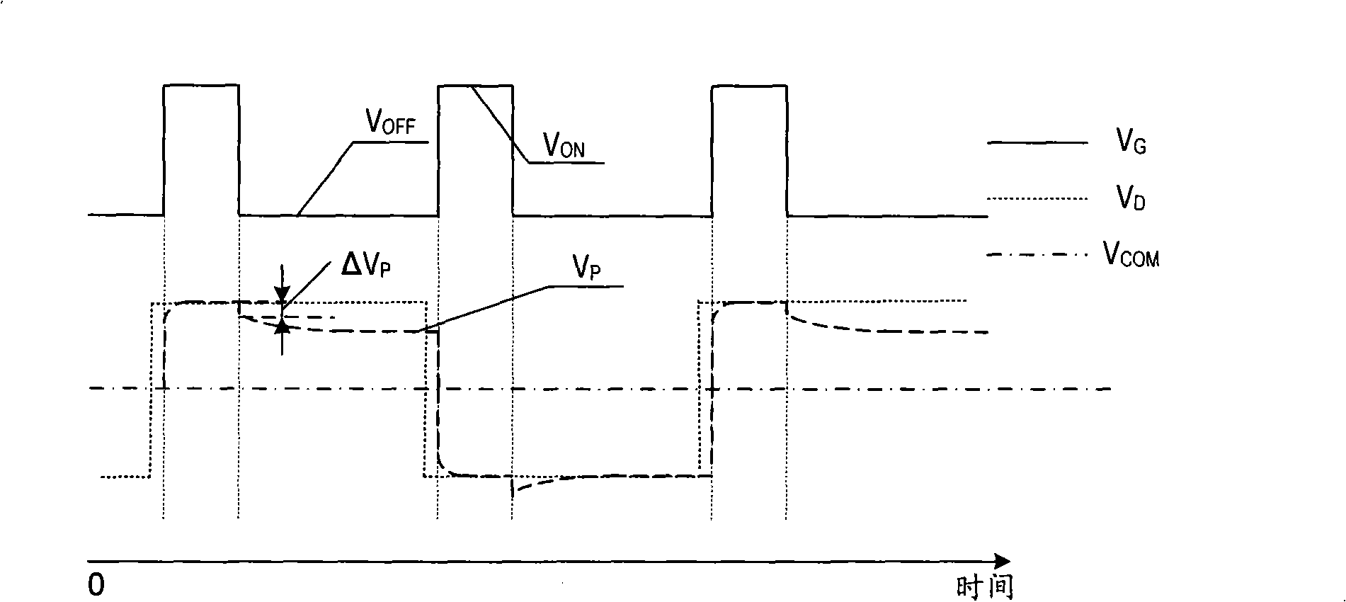
[0065] Image 6 It is a diagram of the second common voltage signal generation mechanism of the present invention, Figure 7 , Figure 8 It is a schematic diagram of the first embodiment of the present invention. In this embodiment, the second common voltage V COM2 It is reversely amplified by the operational amplifier.

[0066] Such as Image 6 As shown, the signal V' is generated by the chip of the PCB circuit board (which can be programmed with Tcon) COM2 , where V′ COM2 Has the following characteristics:

[0067] (1) Signal V' COM2 is a square wave AC signal;

[0068] (2) The lowest value V' COM2L The holding time is t′ 2L , the highest value V′ COM2H The holding time is t′ 2H , and guarantee t′ 2L and t' 2H The sum is the period of the gate signal;

[0069] (3) Signal V' COM2 The falling edge of corresponds to the falling edge of the gate signal;

[0070] (4)t' 2H time at the gate turn-on voltage V ON Within the hold time, the smaller the better.

[007...

no. 2 example

[0079] Figure 9 , Figure 10 It is a schematic diagram of the second embodiment of the present invention. In this embodiment, the second common voltage V COM2 It is amplified by the operational amplifier.

[0080] Such as Image 6 As shown, the chip of the PCB circuit board (which can be programmed with Tcon) generates the signal V″ COM2 , where V″ COM2 Has the following characteristics:

[0081] (1) Signal V″ COM2 is a square wave AC signal;

[0082] (2) The lowest value V″ COM2L The holding time is t” 2L , the highest value V" COM2H The holding time is t” 2H , and guarantee t” 2L and t" 2H The sum is the period of the gate signal;

[0083] (3) Signal V" COM2 The rising edge of corresponds to the falling edge of the gate signal;

[0084] (4)t" 2L time at the gate turn-on voltage V ON Within the hold time, the smaller the better.

[0085] Second common voltage V COM2signal is determined by the above V” COM2 The signal is amplified forward by the operationa...

no. 3 example

[0093] In this embodiment, the second common voltage V COM2 generated by the switching circuit.

[0094] Two variable voltages are generated by two voltage divider resistor circuits: V COM2L and V COM2H , the second common voltage V is controlled by the switching circuit COM2 Signal, which needs to provide switching signal to the switching circuit. When the gate voltage V G by the gate turn-on voltage V ON drops to the gate-off voltage V OFF At the moment, the switch signal is high (or low), and the switch circuit gates V COM2H voltage, the second common voltage V COM2 The voltage of the signal is determined by the V COM2L rise to V COM2H , V COM2H The voltage starts to hold, when the switch signal is low (or high), the switch gates V COM2L voltage, the second common voltage V COM2 The voltage of the signal is determined by the V COM2H down to V COM2L . Among them, the switching signal has the following characteristics:

[0095] (1) The switch signal is a squar...


PUM


Abstract

The invention relates to a TEF-LCD control method which comprises the following steps of exerting a first DC common voltage signal to a common electrode of a substrate of a colored filter, exerting a second square wave AC common voltage signal to a common electrode line of a substrate of an array, a rising edge of the second common voltage signal corresponds to a falling edge of a grid voltage signal, the sum of the holding time of the maximum value and the minimum value of the second common voltage is equal to a cycle of the grid voltage signal, and the holding time of the minimum value of the second common voltage is within the holding time of a grid threshold voltage. At the time when TFT is shut off, the control method can be used to compensate the feedback voltage deltaVP existing in the prior art through the voltage change of the second common voltage so that a pixel voltage VP can not produce the feedback voltage deltaVP, picture flashing and the residual direct voltage are removed, the poor incidental image is improved, the technology for adjusting the common voltage is saved, the yield is improved and poor products due to unadjustable common voltage and so on are avoided.

Description

technical field [0001] The invention relates to a method for providing a common voltage applied to a thin-film transistor liquid crystal display, in particular to a TFT-LCD control method using a color filter substrate and an array substrate to respectively provide a common voltage. Background technique [0002] Thin Film Transistor Liquid Crystal Display (TFT-LCD for short) has two upper and lower substrates (panels): color filter panel (color filter panel, CF substrate for short) and array substrate (array panel, array substrate for short) ), the liquid crystal material is filled between the two substrates, and the liquid crystal material has an anisotropic capacitance value. By applying a common voltage to the transparent electrode ITO coated on the CF substrate and applying a data voltage to the pixels of the array substrate, an electric field is generated between the CF substrate and the Array substrate, and the liquid crystal rotates under the action of the electric fi...

Claims


Application Information

Patent Timeline
Patent Type & Authority Applications(China)
IPC IPC(8): G09G3/36G09G3/20G02F1/133
Inventor 石悦
Owner BOE TECH GRP CO LTD
Why Eureka
Try Eureka