Method for increasing grinding wafer flatness

A flatness and wafer technology, which is applied in the direction of grinding devices, grinding machine tools, electrical components, etc., can solve the problems affecting the flatness of the wafer, affecting the flatness of the center position of the wafer, and increasing production costs, so as to improve production efficiency and uniform grinding force , Improve the effect of flatness

Inactive Publication Date: 2009-02-04
SEMICON MFG INT (SHANGHAI) CORP
View PDF0 Cites 1 Cited by
  • Summary
  • Abstract
  • Description
  • Claims
  • Application Information

AI Technical Summary

Problems solved by technology

[0004] In the prior art, since the grinding head is in the grinding process, the coverage of the grinding head has exceeded the wafer surface, that is, a part of the coverage of the grinding head is not in contact with the grinding disc. When a part of the grinding head is not in contact with the grinding disc When the time is high, the force on the grinding head on the grinding disc will change, that is, the grinding force on the wafer will be uneven, which will affect the flatness of the wafer being ground. Uniformity leads to copper residue at the engraved mark, which causes the wafer to be scrapped due to unclear engraved marks
At present, in order to avoid this situation, it is usually necessary to re-grind the edge of the wafer. However, if the re-grinding operation is not careful, it will affect the flatness of the center of the wafer. In addition, the re-grinding will prolong the grinding time and increase the production cost.

Method used


Image

  • Method for increasing grinding wafer flatness

Examples


Embodiment Construction

[0013] The invention provides a method for improving the flatness of grinding wafers. The method improves the flatness of wafer grinding by adjusting the range of movement of a grinding head in a grinding machine platform.

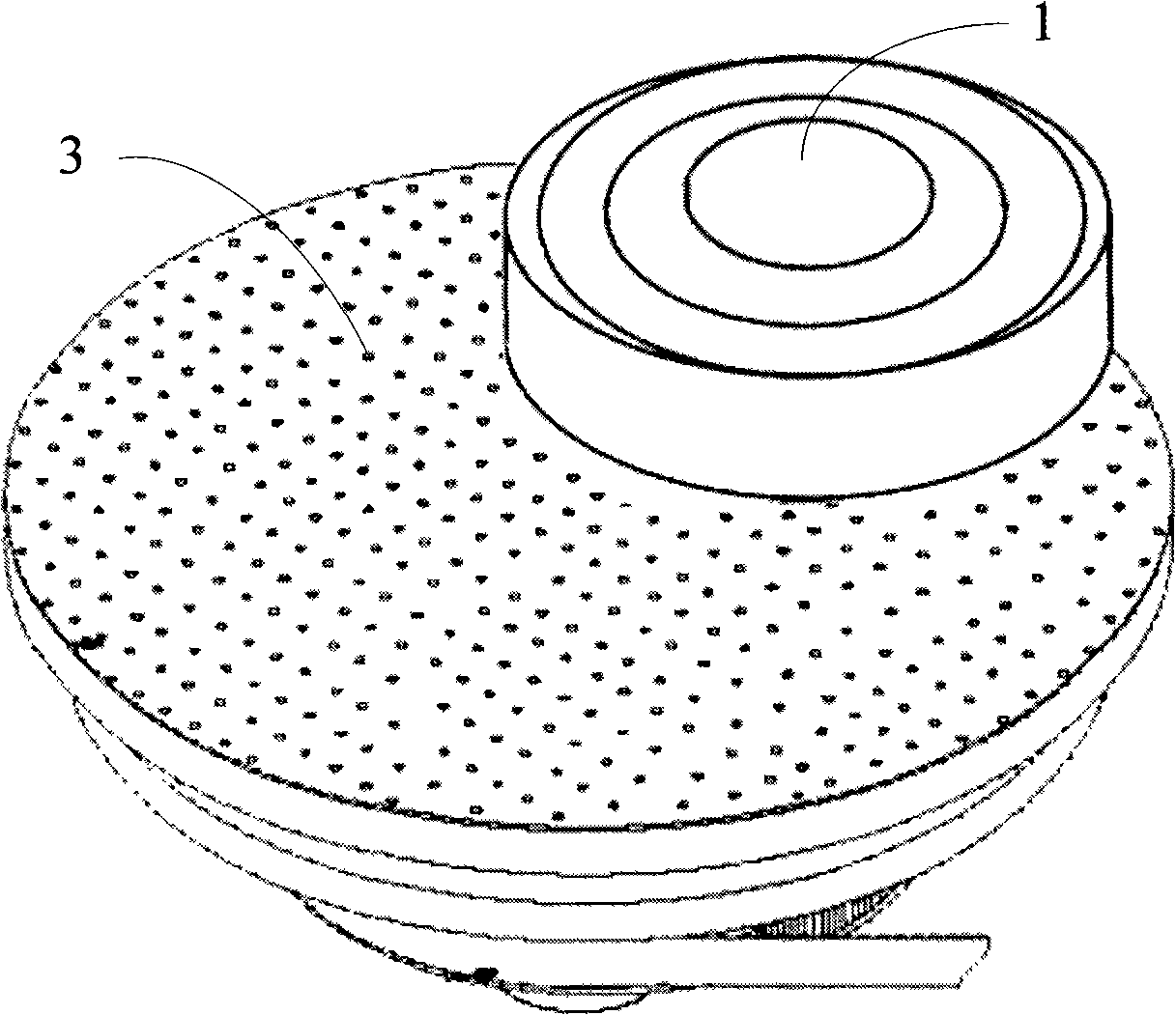
[0014] see figure 1 , the bottom surface of the grinding head 1 is composed of an adsorption portion and a fixed ring. The suction part (not labeled) is used to absorb the wafer (not shown) for grinding, and the fixing ring (not labeled) is used to fix the wafer.

[0015] The grinding disc 3 is used in conjunction with the grinding head 1, and the grinding disc 3 is used for grinding the copper on the surface of the wafer. During the movement of the grinding head 1, the wafer fixing ring of the grinding head 1 should be completely in contact with the grinding disc 3, so as to ensure that the wafer is subjected to a uniform grinding force, thereby ensuring the flatness of the wafer surface.

[0016] In a preferred embodiment of the present invention, the ...


PUM


Abstract

The invention provides a method for improving the planeness of a ground wafer; the method is applied on a grinding machine which comprises a grinding head and a grinding disc; the grinding head is used for adsorbing and fixing the wafer; the grinding disc is used with the grinding head and used for grinding the wafer, wherein, the motion range of the grinding head does not exceed the surface of the grinding disc; the brim of the bottom of the grinding head is provided with a fixing ring which is used for fixing the wafer and is contacted with the grinding disc completely. Compared with the prior art, the even grinding force exerted on the wafer can improve the planeness of the wafer surface in one grinding process and can improve the production efficiency and the yield of the wafer simultaneously.

Description

technical field [0001] The invention relates to a chemical mechanical polishing process, in particular to a method for improving the flatness of a polished wafer. Background technique [0002] At present, copper is used as the metal material of the interconnection structure in integrated circuits, and a dual damascene (Dual Damascene) process is usually used to realize the copper interconnection of the integrated circuit. Using the dual damascene process to manufacture integrated circuit copper interconnection, after filling the copper into the wire trench, chemical mechanical polishing (Chemical Mechanical Polish) will be used to planarize the copper layer, remove excess copper on the dielectric layer, and make the wafer surface fully Permanent planarization for subsequent thin film deposition. [0003] Before the wafer enters the chemical mechanical polishing process, it will be marked to distinguish the wafer. The marking of the wafer is usually set on the edge of the wa...

Claims


Application Information

Patent Timeline
IPC IPC(8): B24B37/04H01L21/304B24B37/07
Inventor 陈肖科黄军平候柏宇马智勇
Owner SEMICON MFG INT (SHANGHAI) CORP
Why Eureka
Try Eureka