Combined through-hole construction for printed circuit board

A printed circuit board, combined technology, applied in the direction of printed circuit components, etc., can solve the problems affecting the transmission quality of differential signal lines, the difficulty of wiring of differential signal lines, etc., to avoid impedance mismatch and electromagnetic interference, and eliminate interference Effect

Active Publication Date: 2009-03-18
珠海芯物科技有限公司
View PDF0 Cites 4 Cited by
  • Summary
  • Abstract
  • Description
  • Claims
  • Application Information

AI Technical Summary

Problems solved by technology

Moreover, since the conductive material in the above-mentioned through-hole area and the differential signal line can generate electromagnetic interference (EMI), thereby affecting the transmission quality of the differential signal line, the differential signal line that originally requires a higher routing path is being routed. becomes more difficult when

Method used


Image

  • Combined through-hole construction for printed circuit board
  • Combined through-hole construction for printed circuit board
  • Combined through-hole construction for printed circuit board

Examples


Embodiment Construction

[0024] Embodiments of the present invention are described below through specific examples, and those skilled in the art can easily understand other advantages and effects of the present invention from the content disclosed in this specification. The present invention can also be implemented or applied through other different specific examples, and various modifications and changes can be made to the details in this specification based on different viewpoints and applications without departing from the spirit of the present invention.

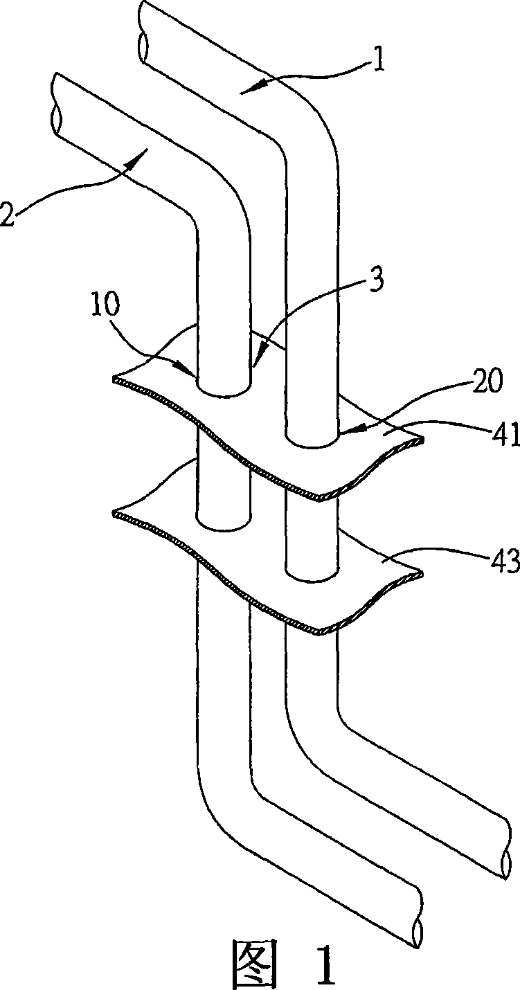
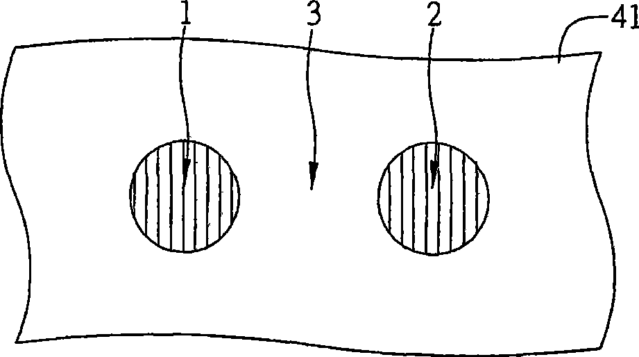
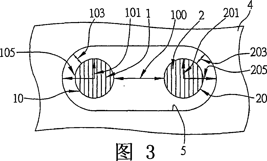
[0025] FIG. 3 is a schematic plan view showing a cross-sectional view of the combined through-hole structure of the printed circuit board of the present invention applied to a printed circuit board (PCB). As shown in the figure, the combined through-hole structure of the printed circuit board of the present invention is required for changing the layer of the combined signal line of a printed circuit board or connecting with other electronic compo...


PUM


Abstract

The invention relates to a combined through-hole construction of printed circuit board, which can be applied to a first, and a second signal line, and a printed circuit board of multi-substrate. The combined through-hole construction includes a first and a second through-hole corresponding to the first and the second signal lines through the multi-substrate spaced by a predetermined distance, and a insulation region corresponding to rim of the first through-hole and the second through-hole. The insulation region includes at least a region extending a first safe distance from the outer edge of the first through-hole, a region extending a second safe distance from the outer edge of the second through-hole, and a region between the first through-hole and the second through-hole. Therefore, unmatched resistance and electromagnetic interference caused by wiring between the first and the second through-holes in prior art is avoided by the insulation region.

Description

technical field [0001] The invention relates to a combined through-hole structure of a printed circuit board, in particular to a combined through-hole structure applied to a printed circuit board (PCB) having at least first and second signal lines and multiple substrates. through-hole structure. Background technique [0002] With the continuous development and improvement of electronic technology, the design of printed circuit boards is also developing towards the common goal of high performance and good quality in the process of constantly discovering and solving problems. Therefore, in the design of printed circuit boards, any improvement, as long as it is beneficial to users, improves product quality and performance, improves functions and other substantive enhancements, is a creation with industrial value and also complies with the patent law. Encourage, protect and utilize the creative spirit. [0003] At present, in the design process of the printed circuit board, ma...

Claims


Application Information

Patent Timeline
Patent Type & Authority Applications(China)
IPC IPC(8): H05K1/02
Inventor 韦启锌范文纲
Owner 珠海芯物科技有限公司
Why Eureka
Try Eureka