Detecting device and detecting method
A detection device and detection card technology, applied in the direction of measuring device, measuring device casing, measuring electricity, etc., to achieve stable inspection, reduce noise, and reduce the possibility of electrostatic damage
- Summary
- Abstract
- Description
- Claims
- Application Information
AI Technical Summary
Problems solved by technology
Method used
Image
Examples
no. 1 approach
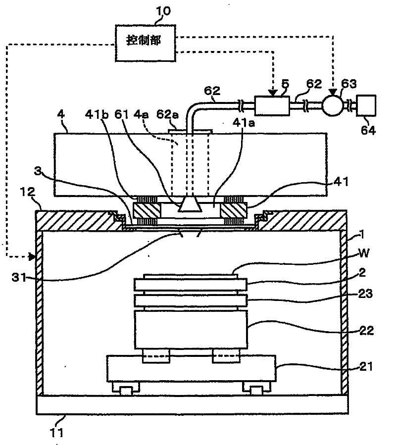
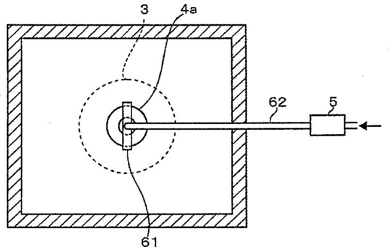
[0053] Such as figure 1 and figure 2 As shown, the detection device according to the embodiment of the present invention includes a housing 1 as an outer casing constituting the main body of the detection device. On the base 11 at the bottom of the frame body 1, there are provided in the following order from the bottom: along the guide rails elongated in the Y direction (the front and back directions of the paper), which are moved along the Y direction by, for example, a ball screw or the like. a driven Y stage 21; and an X stage 22 driven in the X direction by, for example, a ball screw along a guide rail elongated in the X direction. Motors equipped with encoders are respectively provided on the X stage 22 and the Y stage 21, but are omitted here.
[0054]On the X table 22, a Z moving part 23 driven in the Z direction (up and down direction) by an unillustrated motor equipped with an encoder is provided. free to move in the θ direction) as a mounting table wafer chuck 2...
no. 2 approach
[0070] In this embodiment, if Figure 5 As shown, the nozzle part 61 is provided on the mouth edge part of the opening of the top plate 12 for installing the probe card 3 to eject ionized air toward the probe card 3, and the ionizer 5 is connected from the nozzle part 61 to the ion generator 5. The arrangement of the air supply pipe 62 is carried out in the gap between the test head 4 and the top plate 12 . Such a configuration also has the same effect.
no. 3 approach
[0072] As described above, in the previous embodiment, the imaging unit used for the so-called wafer alignment was not shown, but in this embodiment Figure 6 and Figure 7 The overall configuration is described in , and the camera unit is also described. Such as Figure 7 As shown, the micro camera 7 as the first imaging unit is fixed on the Z moving part 23 below the wafer chuck 2 . In addition, at a height position between the wafer chuck 2 and the tip of the probe 31 , a horizontally long angular cylinder-shaped moving body 8 capable of moving horizontally while facing the wafer chuck 2 is provided. The moving body 8 is guided by a guide rail 81 attached to the lower surface of the top plate 12 and is configured to be horizontally movable by a driving device not shown.
[0073] The moving body 8 is provided with a micro camera 82 as a second imaging unit for taking an image of the wafer W, and the moving body 8 is moved to a predetermined alignment position in advance, ...
PUM
 Abstract
Description
Claims
Application Information


