Method of forming a semiconductor die having a sloped edge for receiving an electrical connector

A die, sloping edge technology, used in semiconductor devices, semiconductor/solid-state device manufacturing, semiconductor/solid-state device components, etc., which can solve problems such as increasing package height and offsetting additional occupied area

Inactive Publication Date: 2009-03-25
SANDISK CORP
View PDF1 Cites 4 Cited by
  • Summary
  • Abstract
  • Description
  • Claims
  • Application Information

AI Technical Summary

Problems solved by technology

The package 20 of FIG. 1 allows the die to be stacked directly on top of each other, but the wire bonds 26 still increase the height of the package, and the offset requires additional footprint in the package

Method used


Image

  • Method of forming a semiconductor die having a sloped edge for receiving an electrical connector
  • Method of forming a semiconductor die having a sloped edge for receiving an electrical connector
  • Method of forming a semiconductor die having a sloped edge for receiving an electrical connector

Examples


Embodiment Construction

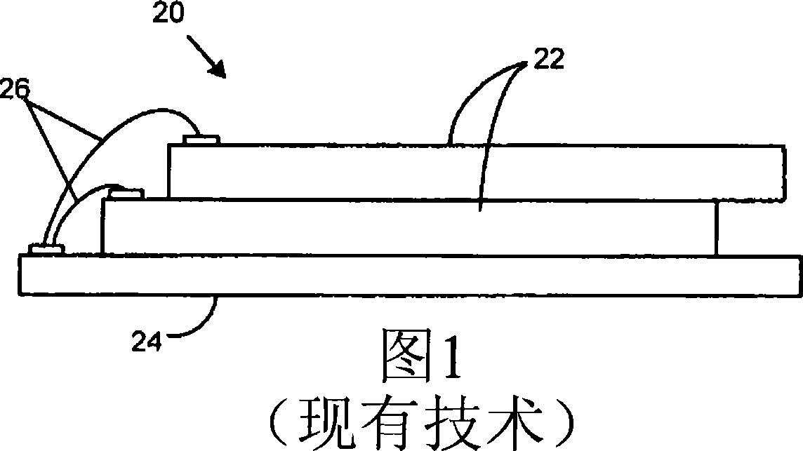
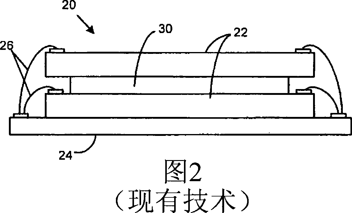
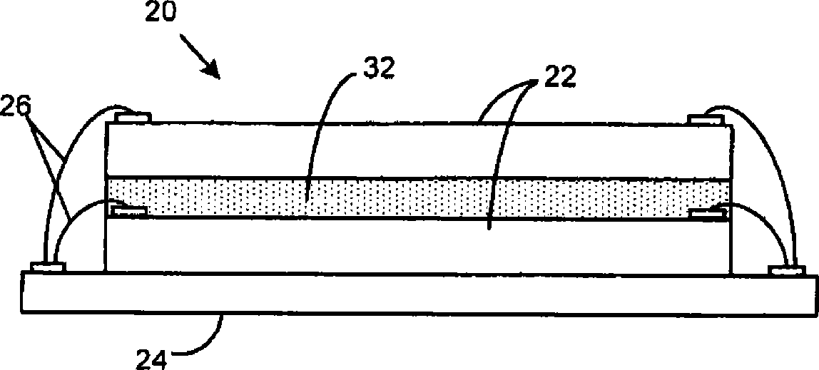
[0029] The embodiments will now be described with reference to FIGS. 4 to 25, which relate to low profile semiconductor packages. It should be understood that the present invention can be implemented in many different forms and should not be construed as being limited to the embodiments set forth herein. In fact, these embodiments are provided so that this disclosure will be thorough and complete, and will fully convey the present invention to those skilled in the art. Indeed, it is hoped that the present invention covers alternatives, modifications and equivalents of these embodiments, which are included in the scope and spirit of the present invention as defined by the appended claims. In addition, in the following detailed description of the present invention, many specific details are set forth in order to provide a thorough understanding of the present invention. However, it will be clear to those skilled in the art that the present invention can be practiced without these sp...


PUM


Abstract

A method of forming a low profile semiconductor package, and a semiconductor package formed thereby, are disclosed. The semiconductor die is formed with one or more sloped edges on which electrically conductive traces may be deposited to allow the semiconductor die to be coupled to another die and / or a substrate on which the die is mounted. Depositing the electrical traces directly on the surface and sloped edge of the die allows the die to be electrically coupled without bond wires, thereby allowing a reduction in the overall thickness of the package.

Description

Technical field [0001] The embodiment of the present invention relates to a low profile semiconductor device and a manufacturing method thereof. Background technique [0002] The significant growth in demand for portable consumer electronic components is driving the need for high-capacity storage devices. Non-volatile semiconductor memory devices, such as flash memory memory cards, are becoming widely used to meet the ever-increasing need for digital information storage and exchange. Its portability, variety and robust design, as well as its high reliability and large capacity have made this type of memory device ideal for use in a variety of electronic devices, including, for example, digital cameras, digital music players, and video game consoles. , PDA and cellular phone. [0003] Although a wide variety of package configurations are known, flash memory memory cards can generally be manufactured as a system in package (SiP) or a multi-chip module (MCM) in which multiple die ar...

Claims


Application Information

Patent Timeline
Patent Type & Authority Applications(China)
IPC IPC(8): H01L21/60H01L23/48H01L25/00H01L25/18
CPCH01L2924/1433H01L23/3121H01L2224/73265H01L25/0657H01L2225/06551H01L2924/01015H01L24/24H01L2224/97H01L2224/48091H01L2224/24145H01L2924/01006H01L2924/01078H01L2224/24051H01L2924/01079H01L21/78H01L2924/14H01L24/25H01L2924/01005H01L2224/32145H01L2225/06562H01L2924/01082H01L2924/01013H01L2924/01003H01L24/82H01L2224/76155H01L2224/82102H01L2924/01029H01L24/97H01L25/50H01L2224/24226H01L2224/24011H01L21/3043H01L2224/48227H01L2924/01033H01L2924/351H01L2924/181H01L2224/05554H01L2924/00014H01L2224/82H01L2924/00H01L2924/00012H01L21/30H01L23/12
Inventor 奇门·于廖智清赫姆·塔基阿尔
Owner SANDISK CORP
Why Eureka
Try Eureka