LED and its making method

A technology of light-emitting diodes and manufacturing methods, which is applied in semiconductor/solid-state device manufacturing, electrical components, electric solid-state devices, etc., and can solve the problems that light-emitting diodes cannot use high brightness, wires 13 are detached, and the defect rate increases.

Inactive Publication Date: 2009-05-06
PROLIGHT OPTO TECH
View PDF0 Cites 0 Cited by
  • Summary
  • Abstract
  • Description
  • Claims
  • Application Information

AI Technical Summary

Problems solved by technology

[0004] In general, a light-emitting diode is placed on a substrate with a single chip, so that the positive and negative poles of the chip are set up, and then the positive and negative poles of the chip are wired to connect the chip to more than one pin. , and then packaged to form a light-emitting diode; and because the light-emitting diode only constitutes a light-emitting diode with a single chip, its light source is not strong, so the above-mentioned conventional light-emitting diodes cannot be used in high-brightness applications.
[0005] Therefore, there are relevant operators who place more than one chip 12 on a substrate 11, as shown in FIG. The positive and negative poles 121, 122 of the positive and negative poles 121, 122 are connected in series by putting wires 13 on them, and then they are packaged to form a light-emitting diode 1; this single light-emitting diode 1 can emit a stronger light source; however, each The connection of multiple wires is required for electrode connection. As shown in the figure, connecting three chips 12 in series requires 4 wires 13 to form an electrical connection. Not only is the manufacturing process more complicated, but also the chances of wires 13 being easily detached due to pulling are also increased. Non-performing rate increased

Method used


Image

  • LED and its making method
  • LED and its making method
  • LED and its making method

Examples


Embodiment Construction

[0029] In order to make your examiner understand the main technical content and implementation mode of the present invention, the description is as follows with the help of drawings:

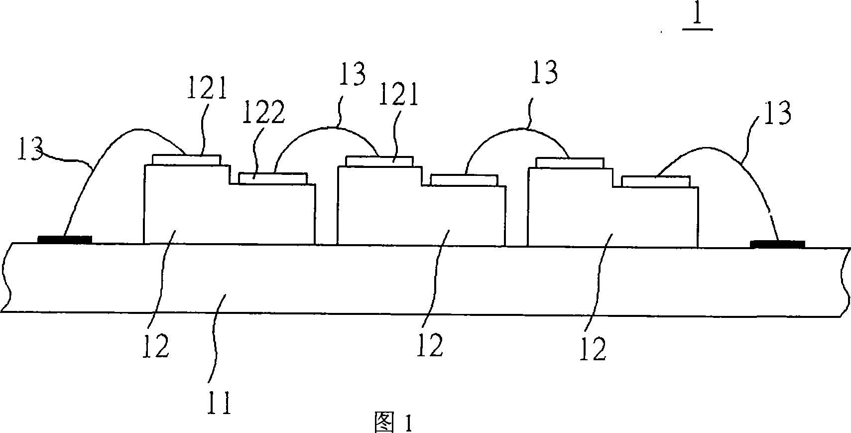
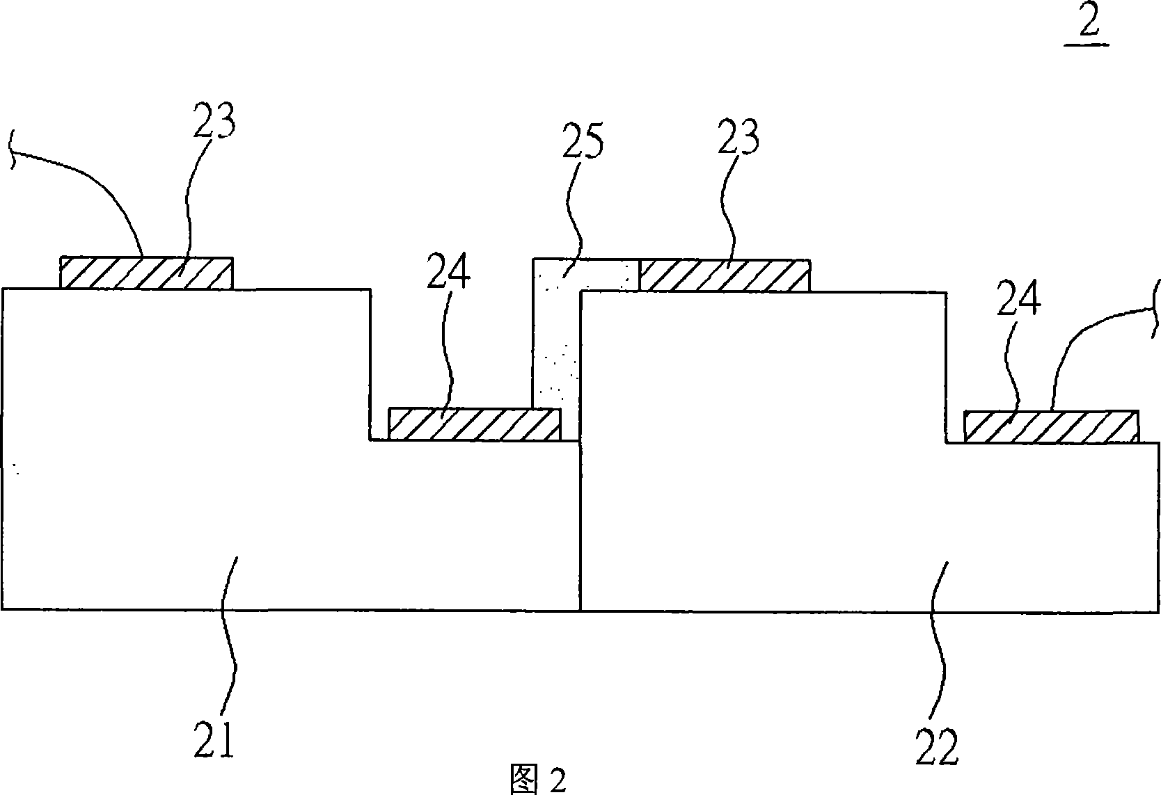
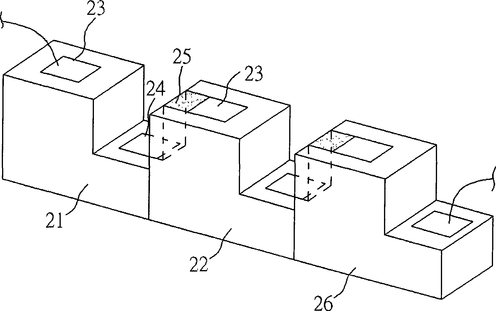
[0030] The light-emitting diode of the present invention and its manufacturing method, as shown in Figure 2, the light-emitting diode 2 is provided with at least a plurality of light-emitting chips, as shown in the figure is provided with first and second light-emitting chips 21,22, each light-emitting chip 21,22 surface There are separated positive and negative poles 23 and 24, and the two light-emitting chips 21 and 22 are arranged continuously, wherein the negative pole 24 of the first light-emitting chip 21 is close to the positive pole 23 of the second light-emitting chip 22, and the positive pole of the first light-emitting chip can also be approached. The negative electrode of the second light-emitting chip.

[0031] Among them, the negative and positive electrodes 24 and 23 of the first ...


PUM


Abstract

A light emitting diode in the invention comprises a plurality of luminescent chips arranged continuously. Detached positive and negative electrodes are arranged on the surface of each luminescent chip; and a conducting channel is connected between the positive and the negative electrodes of the adjacent luminescent chips, so that all the luminescent chips can be connected in series, thereby the whole light emitting diode has higher brightness and can improve the defect of more complicate manufacturing process when the light emitting diodes are connected in series by a lead wire.

Description

technical field [0001] The present invention relates to a light-emitting diode and its manufacturing method, aiming to provide a light-emitting diode and its manufacturing method which can have higher brightness performance and simplify the manufacturing process and only need two wires to complete the connection of each light-emitting chip. Background technique [0002] Press, because light-emitting diodes have absolute advantages compared with traditional light bulbs, such as small size, long life, low voltage / current drive, not easy to break, no significant problems when emitting light, no mercury (no pollution problems), good luminous efficiency ( power saving) and other characteristics, and the luminous efficiency of light-emitting diodes has been continuously improved in recent years, so light-emitting diodes have gradually replaced fluorescent lamps and incandescent bulbs in some fields, such as scanner light sources that require high-speed response, backlights for liqu...

Claims


Application Information

Patent Timeline
IPC IPC(8): H01L25/00H01L25/075H01L23/488H01L21/60
CPCH01L2224/48091
Inventor 邢陈震洪荣豪邢陈震
Owner PROLIGHT OPTO TECH
Why Eureka
Try Eureka