Pixel structure and method of manufacture

A technology of pixel structure and pixel electrode, which is applied in semiconductor/solid-state device manufacturing, photolithographic process exposure device, optics, etc. It can solve the problems of decreased aperture ratio, affecting brightness performance, and enhanced crosstalk effect, so as to improve aperture ratio, The effect of increasing brightness performance and reducing coverage area

Inactive Publication Date: 2012-11-21
INNOLUX CORP
View PDF0 Cites 0 Cited by
  • Summary
  • Abstract
  • Description
  • Claims
  • Application Information

AI Technical Summary

Problems solved by technology

However, due to the increase in the size of the display panel and the increase in the signal transmission frequency, the crosstalk effect is enhanced, so the distance d2 must be increased accordingly.
Similarly, the distance d1 of the scanning line 1 must also be increased, which further leads to a decrease in the aperture ratio and affects the brightness performance

Method used


Image

  • Pixel structure and method of manufacture
  • Pixel structure and method of manufacture
  • Pixel structure and method of manufacture

Examples


Embodiment 1

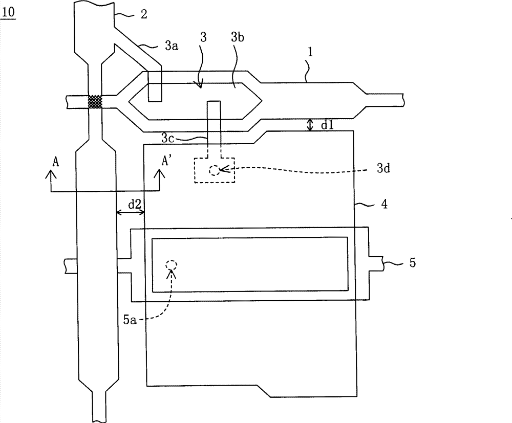
[0058] Please refer to Figure 2A, which is a schematic diagram of a pixel structure according to Embodiment 1 of the present invention. The pixel structure 100 includes scan lines 110 , data lines 120 , thin film transistors 130 , pixel electrodes 140 and storage capacitors 150 . The thin film transistor 130 is disposed on the scan line 110, and a part of the scan line 110 is used as the gate 130e of the thin film transistor 130 to control its switching. The data line 120 is coupled to the source 130a of the thin film transistor 130. When an appropriate voltage is applied to the scanning line 110, the signal can be transmitted through the channel layer 130b, and output from the drain 130c to the pixel electrode 140 through the contact hole 130d. The storage capacitor 150 is coupled to the pixel electrode 140 through the contact hole 150 a for maintaining the voltage of the pixel electrode 140 .

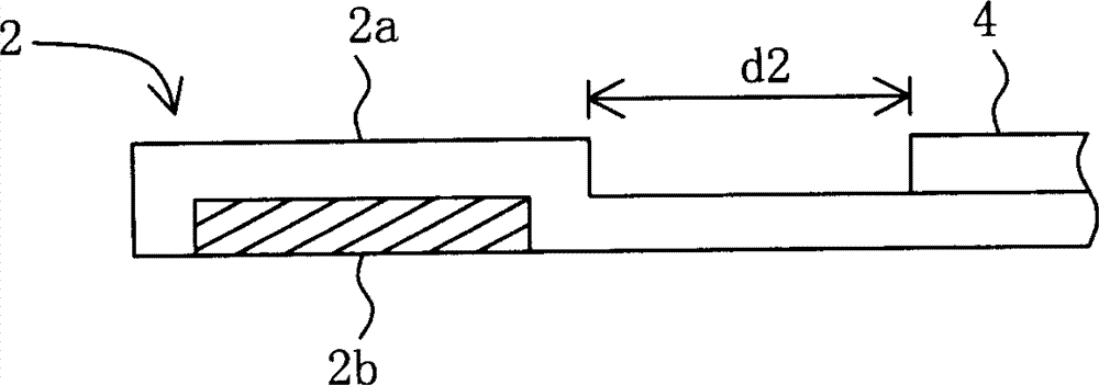
[0059] Please refer to Figure 2B , which is shown as Figure 2A The cross-s...

Embodiment 2

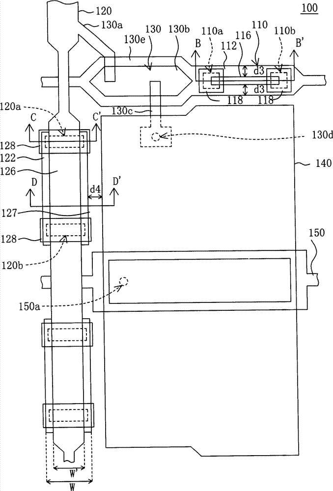
[0080] Please refer to Figure 7A , which is a schematic diagram of a pixel structure in Embodiment 2 of the present invention. The main difference between the pixel structure 200 and the pixel structure 100 of the first embodiment lies in the types of the contact holes in the scan line 210 and the data line 220, and the rest of the elements are the same as those of the first embodiment, and their labels will continue to be used and will not be repeated. The link is off.

[0081] Please refer to Figure 7B , which shows Figure 7A The cross-sectional view of the middle scan line along the section line EE'. The first scanning insulating layer 213 and the second scanning insulating layer 217 respectively have a first contact hole 210a and a second contact hole 210b, and the third scanning metal layer 218 is respectively connected to the first contact hole 210a and the second contact hole 210b. One end of the scanning metal layer 112 and the second scanning metal layer 116 . ...


PUM

PropertyMeasurementUnit
widthaaaaaaaaaa

Abstract

The present invention discloses a picture element structure, which is characterized in that the picture element structure includes a thin-film transistor, a picture element electrode and a scan line. The thin-film transistor is provided with a gate, a source and a drain, and the picture element electrode is coupled with the drain. The scan line includes a first scan metallic layer, a first scan insulation layer, a second scan metallic layer and a third scan metallic layer. The first scan metallic layer is connected with the gate, the first scan insulation layer is arranged at the first scan metallic layer, and the second metallic layer is arranged on the first scan insulation layer. The second scan insulation layer is arranged on the second scan metallic layer, the third scan metallic layer is connected with the first scan metallic layer and the second scan metallic layer. The opening rate of the integral picture element structural can be improved.

Description

technical field [0001] The present invention relates to a pixel structure and its manufacturing method, and in particular to a pixel structure capable of increasing aperture ratio and its manufacturing method. Background technique [0002] With the demand of the market, the size of the display panel is continuously increasing, and the data transmission frequency is increased in response to the high image quality, resulting in more obvious loss of signal transmission, resulting in uneven brightness of the picture (uniformity). In order to improve this problem, the cross-sectional area of ​​the signal line must be increased to reduce signal attenuation. Please refer to Figure 1A , which is a schematic diagram of a pixel structure of a conventional liquid crystal display device. The pixel structure 10 mainly includes a scan line 1 , a data line 2 , a thin film transistor 3 , a pixel electrode 4 and a storage capacitor 5 . The thin film transistor 3 is disposed on the scannin...

Claims


Application Information

Patent Timeline
Patent Type & Authority Patents(China)
IPC IPC(8): G02F1/1362G02F1/133G03F7/20H01L21/027
Inventor 陈建宏
Owner INNOLUX CORP
Why Eureka
Try Eureka