Coated glass pane
A glass plate, coating technology, applied in the direction of thin material handling, transportation and packaging, etc., can solve the problem of unsatisfactory resistance to mechanical and chemical influences, etc.
- Summary
- Abstract
- Description
- Claims
- Application Information
AI Technical Summary
Problems solved by technology
Method used
Image
Examples
Embodiment 1
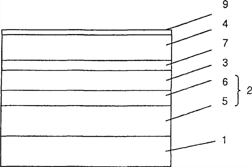
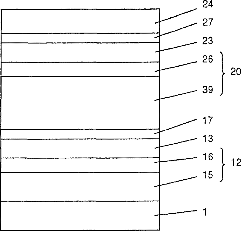
[0102] In a sputtering device with several independent sputtering chambers, a coating containing several layers shown in Table 1 below was deposited on the glass plate, and the following targets or target pairs were set in the chambers:
[0103] (1) The first target pair, including:
[0104] (a) Metal-doped silicon target (with SIPA TM 10 is commercially available from W.C. Heraeus), which contains about 10 wt.% Al as the main dopant, and
[0105] (b) Ceramic aluminum-doped zinc oxide target (with ZAO TM Commercially available from W.C. Heraeus), which contains about 2wt.% Al 2 O 3 ;
[0106] (2) Zinc target;
[0107] (3) Silver target;
[0108] (4) The second target pair, including
[0109] (a) Ceramic TiO x Target (x x CLATO TM Commercially available from W.C. Heraeus)
[0110] (b) Ceramic ZnO:Al target (with ZAO TM Commercially available from W.C. Heraeus), which contains about 2wt.% Al 2 O 3 .
[0111] The sputtering device allows the glass plate to be moved at a controlled rate rel...
Embodiment 2
[0121] A coating having substantially the same layer sequence and thickness as in Example 1 was deposited. However, the difference from Example 1 is that the compound layer is deposited by moving the substrate about 4 times faster under the Al-doped Si(Si:Al) / Al-doped ZnO(ZnO:Al) target pair , And by correspondingly adopting 8-16-8 movement to deposit 3 compound layers with a total thickness substantially the same as that of Example 1. Table 3 summarizes the deposition conditions:
[0122] table 3
[0123] Attached drawing
mark
Target composition Power
[kW] Power
Types of Ar
[sccm] N 2
[sccm] O 2
[sccm] Rate
[mm / min] Move
frequency
15Si:Al /
ZnO:Al
10 / 2
Pulsed DC
200
150
-
3284
8 16 Zn14 Direct current140-45059001 13 Ag1.5 Direct current250--18751
17TiO x /
ZnO:Al
3 / 3
Pulsed DC
175-
-
967
1
39Si:Al /
ZnO:Al
10 / 2
Pulsed DC
200
150-
3284
16 26 Zn14 Direct current140-450...
Embodiment 4-9 and comparative example 10
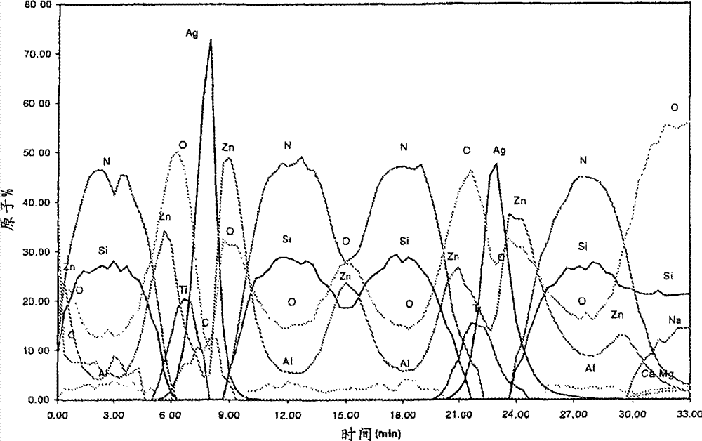
[0139] In another series of experiments, the Si:Zn atomic ratio in the compound layer of the coating with a layer sequence similar to that of Example 1 was changed, in addition to the following differences:
[0140] -Set the thickness of the compound layers 15, 39 and 24 in the coating of the present invention and the thickness of the (aluminum-doped) silicon nitride layer in the comparative coating of Comparative Example 10 to 40, 80, and 40 nm respectively (as compared with the example 1 compared with 35, 70 and 35nm in Comparative Example 3), 2-4-2 movement is achieved under the target at a slightly reduced rate.
[0141] -The power ratio of the Si:Al / ZnO:Al targets used to deposit the compound layers 15, 39 and 24 of another embodiment of the invention varies between 15:2 (Example 4) and 15:8 (Example 9) Therefore, the Si:Zn atomic ratio shown in the second column of Table 5 (derived from XPS analysis) (compared to approximately 2:1 in Examples 1 and 2) is achieved in these lay...
PUM
| Property | Measurement | Unit |
|---|---|---|
| thickness | aaaaa | aaaaa |
| thickness | aaaaa | aaaaa |
| thickness | aaaaa | aaaaa |
Abstract
Description
Claims
Application Information


