Flat panel display device and manufacturing method thereof
A flat-panel display and manufacturing method technology, applied in nonlinear optics, instruments, optics, etc., can solve problems such as the influence of the bonding relationship of liquid crystal displays, and achieve the effect of simplifying the finishing and connection procedures and reducing the overall weight
- Summary
- Abstract
- Description
- Claims
- Application Information
AI Technical Summary
Problems solved by technology
Method used
Image
Examples
Embodiment Construction
[0055] The present invention provides a flat-panel display device and a manufacturing method thereof. The flat-panel display device disclosed in the following embodiments is a liquid crystal flat-panel display device, but is not limited thereto; in different embodiments, the flat-panel display device may also include organic light emitting diodes ( Organic Light Emitting Diode) display device. In addition, the flat panel display device of the present invention includes a back cover set, wherein the back cover set is made in a divided manner and includes a main back cover and at least one sub-back cover.
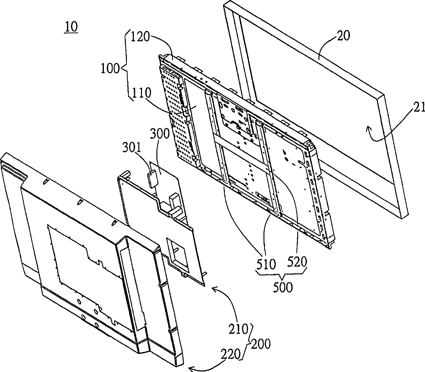
[0056] figure 1 Shown is an exploded perspective view of the first embodiment of the flat panel display device 10 of the present invention. like figure 1 As shown, the flat display device 10 includes a flat display module 100 , a front cover 20 , an auxiliary bracket 500 , a rear cover set 200 and a first circuit board 300 . The back cover assembly 200 is further composed ...
PUM
 Abstract
Description
Claims
Application Information


