LED chip base using diamond film as heat sink material and preparation method
A technology of LED chip and diamond film, applied in electrical components, circuits, semiconductor devices, etc., to achieve the effects of less stringent control requirements, high hardness, and improved work efficiency
- Summary
- Abstract
- Description
- Claims
- Application Information
AI Technical Summary
Problems solved by technology
Method used
Image
Examples
Embodiment 1
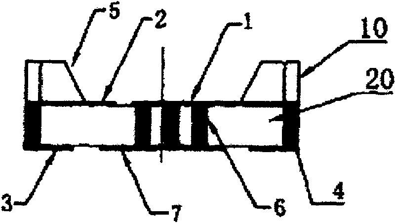
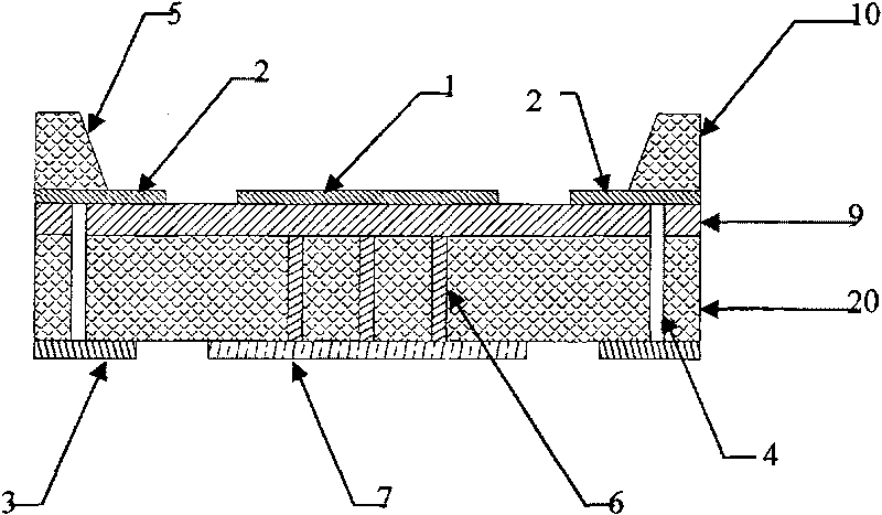
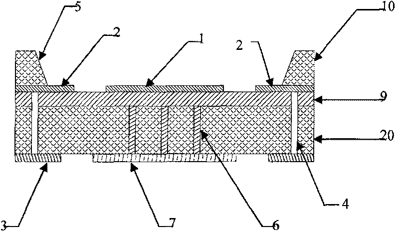
[0022] The structure of the ceramic LED packaging base of the present invention is as follows: figure 2 As shown, 1 is the patch area, 2 is the electrode bonding area, 3 is the bottom pad, 4 is the electrical conduction hole, 5 is the reflector cup, 6 is the heat conduction column, 7 is the heat dissipation pad, 9 is the diamond film, 10 20 is the upper ceramic layer, and 20 is the lower ceramic layer.
Embodiment 2
[0024] in Al 2 o 3 A diamond film was deposited on a ceramic base, prepared by microwave plasma CVD (MPCVD). Specific steps are as follows:
[0025] The first step is to Al of the LED chip 2 o 3 The ceramic substrate (lower ceramic layer 20 ) is firstly cleaned, and ultrasonically cleaned with acetone and alcohol for 5 minutes respectively.
[0026] The second step is in Al 2 o 3 A layer of AlN film with high thermal conductivity is plated on the ceramic substrate by magnetron sputtering as a transition layer to prevent the growing diamond film from Al 2 o 3 Peel off the ceramic. Sputtering target uses Al target, atmosphere N 2 And Ar gas, the pressure is 1-3Pa, the power is 80-150W, and the time is 5-60min.
[0027] In the third step, the Al coated with AlN film 2 o 3 The ceramic substrate is placed in the CVD diamond film growth reaction chamber, and the reaction gas methane and hydrogen are introduced. The pressure in the reaction chamber is 6k-15kPa, the power ...
Embodiment 3
[0030] A diamond film was deposited on an AlN ceramic pedestal, prepared by microwave plasma CVD (MPCVD). Specific steps are as follows:
[0031] The first step is to clean the AlN ceramic substrate (lower ceramic layer 20) of the LED chip, ultrasonically clean it with acetone and alcohol for 5 minutes, and then grind it with diamond powder or abrasive paste with an average particle size of 0.5 μm. Make uniform scratches on the surface and leave some diamond particles to improve the nucleation rate of the diamond film.
[0032] In the second step, the AlN ceramic substrate is placed in the CVD diamond growth reaction chamber, and the reaction gas methane and hydrogen are introduced. The pressure in the reaction chamber is 6k-15kPa, and the power is 1000-3000W. 2 The flow rate is 500 sccm, the methane flow rate is 10-30 sccm, and the substrate temperature is 700-900°C. The film growth rate is 1-20μm / h, and the growth time is 10-200 hours.
[0033] In the third step, after th...
PUM
 Abstract
Description
Claims
Application Information
 - R&D
- Intellectual Property
- Life Sciences
- Materials
- Tech Scout
- Unparalleled Data Quality
- Higher Quality Content
- 60% Fewer Hallucinations
Browse by: Latest US Patents, China's latest patents, Technical Efficacy Thesaurus, Application Domain, Technology Topic, Popular Technical Reports.
© 2025 PatSnap. All rights reserved.Legal|Privacy policy|Modern Slavery Act Transparency Statement|Sitemap|About US| Contact US: help@patsnap.com


