Inner buried type circuit board and method for producing the same

A manufacturing method and circuit board technology, applied in printed circuit manufacturing, removal of conductive materials by chemical/electrolytic methods, printed circuits, etc., can solve problems such as increased load-carrying area, improve performance, reduce size, and improve overall production efficiency Effect

Inactive Publication Date: 2009-07-01
UNIMICRON TECH CORP
View PDF0 Cites 4 Cited by
  • Summary
  • Abstract
  • Description
  • Claims
  • Application Information

AI Technical Summary

Problems solved by technology

In these electronic products, a circuit substrate is usually arranged. In addition to having a conductive circuit, the circuit substrate can also carry a single electronic component such as a capacitor, an inductor, a resistor, or an IC chip as a data processing unit of the electronic product. However, the electronic The arrangement of components or conductive lines on the circuit substrate will increase the carrying area, so how to embed electronic components and conductive lines in the circuit substrate has become a key technology at present

Method used


Image

  • Inner buried type circuit board and method for producing the same
  • Inner buried type circuit board and method for producing the same
  • Inner buried type circuit board and method for producing the same

Examples


Embodiment Construction

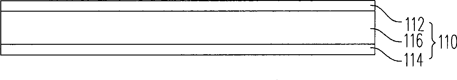
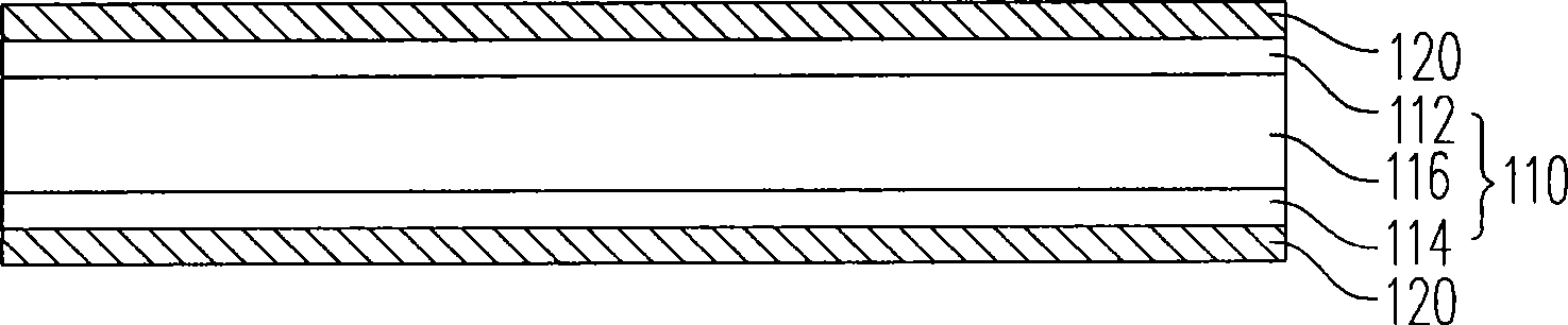
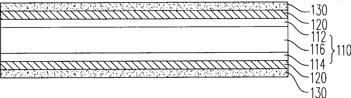
[0036] Figure 1A to Figure 1K A cross-sectional view showing the process of a method for manufacturing an embedded circuit board according to an embodiment of the present invention. The manufacturing method of the embedded circuit board of the present embodiment comprises the following steps: first, as Figure 1A As shown, a composite carrier 110 is provided. The composite carrier 110 includes a first carrier 112, a second carrier 114, and a third carrier 116. The first carrier 112 and the second carrier 114 are located on the third carrier 116 respectively. on both sides. Next, if Figure 1B to Figure 1F As shown, the circuit layer 120' is formed on the first carrier 112 and the second carrier 114 respectively. Hereinafter, this embodiment will firstly describe the formation method of the circuit layer 120' in detail.

[0037]Based on the above, in this embodiment, the method of forming the circuit layer 120 ′ on the first carrier 112 and the second carrier 114 includes t...


PUM


Abstract

The invention discloses an embedded circuit board, which comprises a dielectric layer, two line layers and an electronic component. The line layers are embedded on two side edges of the dielectric layer respectively. Furthermore, the electronic component is embedded in the dielectric layer and electrically connected with one of the line layers. In addition, the invention further discloses a method for manufacturing the embedded circuit board.

Description

technical field [0001] The present invention relates to a circuit board and its manufacturing method, and in particular to an embedded circuit board and its manufacturing method. Background technique [0002] In recent years, with the rapid development of electronic technology and the emergence of high-tech electronic industries, electronic products with more humanization and better functions are constantly being introduced, and are designed towards the trend of light, thin, short and small. In these electronic products, a circuit substrate is usually arranged. In addition to having a conductive circuit, the circuit substrate can also carry a single electronic component such as a capacitor, an inductor, a resistor, or an IC chip as a data processing unit of the electronic product. However, the electronic The arrangement of components or conductive circuits on the circuit substrate will increase the bearing area. Therefore, how to embed electronic components and conductive ci...

Claims


Application Information

Patent Timeline
Patent Type & Authority Applications(China)
IPC IPC(8): H05K3/32H05K3/20H05K3/06H05K1/16
Inventor 张振铨
Owner UNIMICRON TECH CORP
Why Eureka
Try Eureka