
Optically controlled silicon carbide and related wide-bandgap transistors and thyristors

A silicon carbide layer, field effect transistor technology, applied in electrical components, semiconductor devices, climate sustainability, etc., can solve problems such as half-bridge misoperation, low thermal conductivity, increased system complexity and cost, etc.

Inactive Publication Date: 2011-07-27
PI
View PDF8 Cites 0 Cited by
  • Summary
  • Abstract
  • Description
  • Claims
  • Application Information

AI Technical Summary

Problems solved by technology

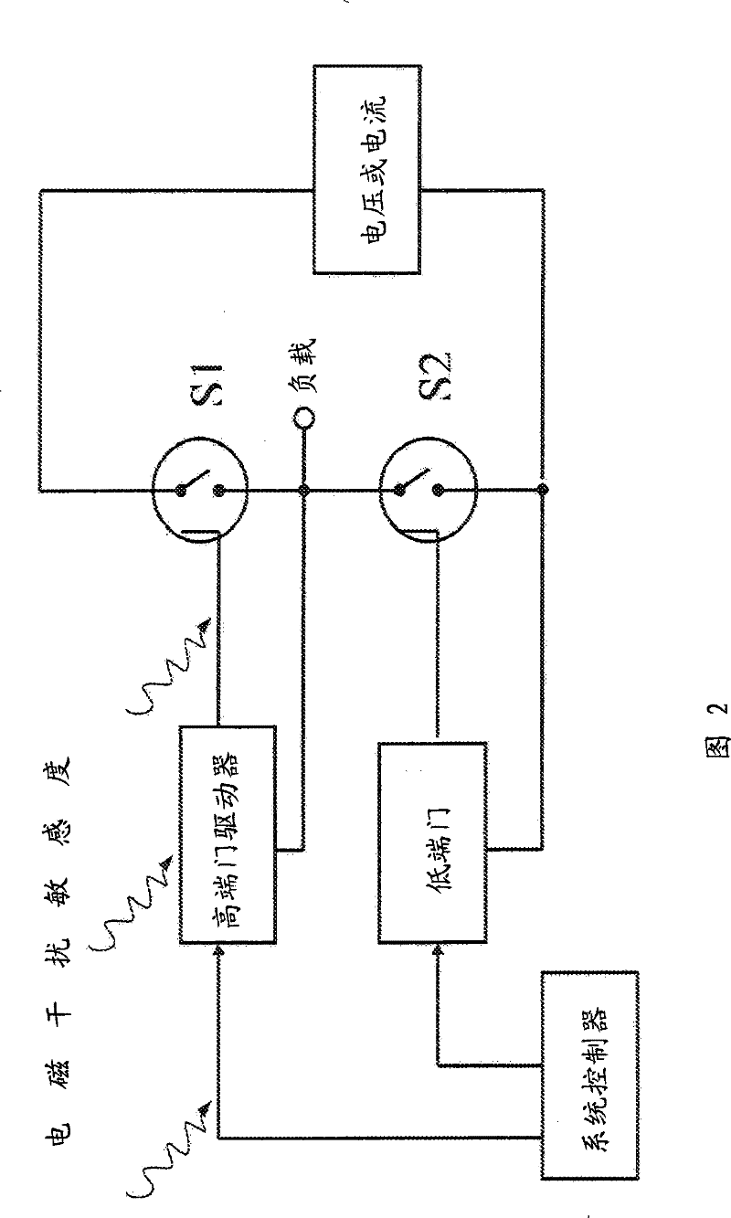
The first disadvantage is the "high-side gate driver" problem: the upper switch S1 is electrically controlled by the gate driver circuit with which the load is connected in common, therefore, a floating gate drive is required
This increases system complexity and cost
The second problem is the possibility of generating false gate signals that can cause erroneous operation of the half-bridge, which can lead to failure of the circuit or load
Another disadvantage is that GaAs is usually rarely used in the power electronics industry because of its low thermal conductivity, etc.
Schoenbach et al. did not give a better choice of semiconductors that can be practically applied to power electronics, such as silicon carbide

Method used


Image

  • Optically controlled silicon carbide and related wide-bandgap transistors and thyristors
  • Optically controlled silicon carbide and related wide-bandgap transistors and thyristors
  • Optically controlled silicon carbide and related wide-bandgap transistors and thyristors

Examples


Embodiment Construction

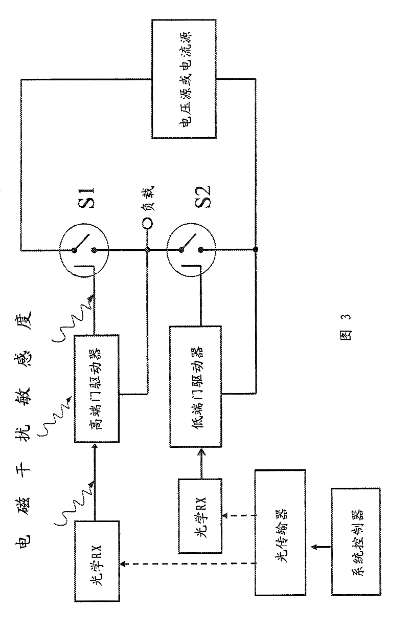
[0038] The present invention provides silicon carbide photoactive materials for use in the fabrication of a whole class of power devices and integrated circuits, with significant advantages in circuits requiring or benefiting from pure optical gate control. One implementation of this application is as Figure 7 Circuit 1 is shown. The circuit is a half-bridge power circuit comprising two transistor switches 2, one in the "high side" position and the other in the "low side" position. The controller 3 drives a source of electromagnetic radiation 4 capable of producing a beam of electromagnetic radiation 5 at a first wavelength and a beam 6 of electromagnetic radiation at a second wavelength, the first wavelength being smaller than the second wavelength. The high side switch and the low side switch may be illuminated with any of an arbitrary sequence of beams determined by the controller. Such half-bridge circuits are themselves used in various power supplies or as output stage...


PUM


Abstract

An optically active material is used to create power devices and circuits having significant performance advantages over conventional methods for affecting optical control of power electronics devices and circuits. A silicon-carbide optically active material is formed by compensating shallow donors with the boron related D-center. The resulting material can be n-type or p-type but it is distinguished from other materials by the ability to induce persistent photoconductivity in it when illuminated by electromagnetic radiation with a photon energy in excess of the threshold energy required to photoexcite electrons from the D-center to allowed states close to the conduction band edge, which varies from polytype to polytype.

Description

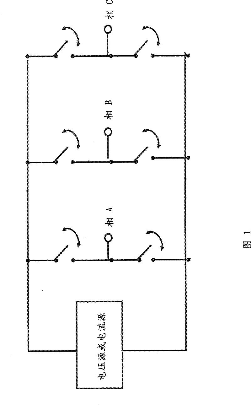
technical field [0001] The present invention relates to an advanced microelectronic (semiconductor) device and method of manufacturing the same, and in particular to a microelectronic device comprising a region of photoactive material that causes the device to be turned off by a pulse of light at one wavelength and then It is turned on by light pulses of two wavelengths. Background technique [0002] like figure 1 The circuit shown is used in a wide variety of devices needed to convert one voltage or current (usually DC) to a three-phase AC voltage or current (and vice versa). Such as motor drives for electric vehicles, industrial motors for factory use, utility power conditioning systems, such Static Volt-Ampere Response (SVAR) compensators, rectifiers and converters for high-voltage DC power transmission, the two-switch and four-switch types of the Circuits (referred to as "half-bridge" and "full-bridge", respectively) are widely used in power supply in the defense and c...

Claims


Application Information

Patent Timeline
Patent Type & Authority Patents(China)
IPC IPC(8): H01L31/10H01L31/16H02M7/00
CPCY02B70/1483
Inventor 迈克尔·S·马佐拉
Owner PI
Learn More