Optically controlled silicon carbide and related wide-bandgap transistors and thyristors

a wide-bandgap transistor and thyristor technology, applied in the field of advanced microelectronic (semiconductor) devices, can solve the problems of increasing complexity and cost in the final system, failure to occur in either the circuit or the load, and additional threat of intentionally introduced emi from enemy action

Inactive Publication Date: 2014-10-07
POWER INTEGRATIONS INC
View PDF34 Cites 4 Cited by
  • Summary
  • Abstract
  • Description
  • Claims
  • Application Information

AI Technical Summary

Benefits of technology

[0017]In another embodiment, the optically active material formed by D-center compensated SiC is incorporated into the channel of optically controllable vertical and lateral channel junction field effect transistors (JFET

Problems solved by technology

This introduces greater complexity and cost into the final system.
The second problem is the possible introduction of incorrect gate signals which could cause improper operation of the half-bridge, possibly causing a failure to occur in either the circuit or the load.
But in military related systems, there is the additional threat of intentionally introduced EMI from enemy action.
Unfortunately, the problem of providing isolated electrical power to the receiver and the gate driver remains.
And the gate driver circuitry is still potentially vulnerable to EMI.
The former problem is especially troublesome whenever a long string of devices are connected in series to multiply the total blocking voltage of the stack, as is often the case in electric utility equipment.
The principal limitation is that the switch cannot usually be switched off with light, which accounts for the popularity of thyristors because they can generally be switched off by the external circuit through a process known as commutation.
This limits the optically triggered thyristor, by far the most commonly used optically active switch used in power electronics, to applications where circuit commutation is possible; however, in many applications commutation is not an option which severely limits the application of the prior art in optically active switches.
When the light is removed, the BJT will stop conducting current and in due course the switch will turn off or “open.” The proble

Method used


Image

  • Optically controlled silicon carbide and related wide-bandgap transistors and thyristors
  • Optically controlled silicon carbide and related wide-bandgap transistors and thyristors
  • Optically controlled silicon carbide and related wide-bandgap transistors and thyristors

Examples


Embodiment Construction

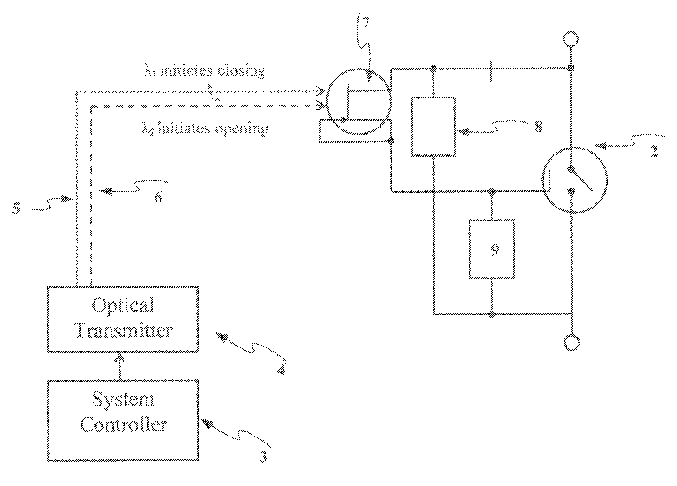
[0039]The present invention provides for a silicon carbide optically active material used to create an entire class of power devices and integrated circuits with significant advantages in circuits requiring or benefiting from control by pure optical gating. An example of one such application is the circuit 1 shown in FIG. 7. The circuit is a half-bridge power circuit containing two transistor switches 2, one in the “high side” position and one in the “low side” position. A controller 3 drives a source of electromagnetic radiation 4 which can produce beams of electromagnetic radiation of one wavelength 5 and of a second wavelength 6 such that the first wavelength is less than the second wavelength. Both the high-side and the low-side switches can be illuminated with either of the beams in arbitrary sequences as determined by the controller. Such half-bridge circuits would have application by themselves in various electrical power supplies, or as output stages in integrated circuits. ...


PUM


Abstract

An optically active material is used to create power devices and circuits having significant performance advantages over conventional methods for affecting optical control of power electronics devices and circuits. A silicon-carbide optically active material is formed by compensating shallow donors with the boron related D-center. The resulting material can be n-type or p-type but it is distinguished from other materials by the ability to induce persistent photoconductivity in it when illuminated by electromagnetic radiation with a photon energy in excess of the threshold energy required to photoexcite electrons from the D-center to allowed states close to the conduction band edge, which varies from polytype to polytype.

Description

CROSS REFERENCE TO RELATED APPLICATIONS[0001]This application is a continuation of U.S. patent application Ser. No. 13 / 463,031, filed on May 3, 2012, now allowed, which is a divisional of U.S. patent application Ser. No. 11 / 764,606, filed on Jun. 18, 2007, now U.S. Pat. No. 8,193,537, which claims the benefit of Provisional U.S. Application Ser. No. 60 / 805,139, filed on Jun. 19, 2006. Each of the above applications is incorporated by reference herein in its entirety.BACKGROUND[0002]1. Field[0003]This invention relates to advanced microelectronic (semiconductor) devices and methods for fabricating the same, and in particular, to microelectronic devices containing a region of optically active material that permits the device to be closed with a pulse of light of one wavelength; and then opened with a pulse of light of a second wavelength.[0004]2. Background of the Technology[0005]The circuit shown in FIG. 1 is widely used in diverse applications where the conversion of one voltage or ...

Claims


Application Information

Patent Timeline
IPC IPC(8): H01L29/15H01L31/028H01L31/0312H01L31/09H01L31/11H03K17/78
CPCH01L31/028H03K17/78H01L31/0312H01L31/09H01L31/1105Y10S438/917Y10S438/931H01L31/10H01L31/16H02M7/00
Inventor MAZZOLA, MICHAEL, S.
Owner POWER INTEGRATIONS INC
Why Eureka
Try Eureka