Structure and method for multiple threshold voltage definition in advanced CMOS device technology

a technology of cmos and threshold voltage, applied in the field of semiconductor structure, can solve the problems of less desired channel doping, more difficult to obtain varying threshold voltages for a multitude of devices in a chip, and a resurfacing of fully-depleted device technology, so as to facilitate the action and facilitate the action

Active Publication Date: 2018-09-27
IBM CORP
View PDF11 Cites 5 Cited by
  • Summary
  • Abstract
  • Description
  • Claims
  • Application Information

AI Technical Summary

Benefits of technology

[0004]Principles of the invention, in accordance with one or more embodiments thereof, provide semiconductor structures and methods of obtaining a plurality of fin-type field-effect transistor (FinFET) devices having different discrete threshold voltages by the careful configuration of gate stack material and a channel in the semiconductor structure.
[0005]In accordance with one aspect, an exemplary method for fabricating a semiconductor structure having multiple defined threshold voltages includes: forming a plurality of field-effect transistor (FET) devices in the semiconductor structure, each of the FET devices comprising a channel and a gate stack formed of one of at least two different work function metals, the gate stack being formed proximate the channel; and varying a bang-gap of the channel in each of at least a subset of the FET devices by controlling a percentage of one or more compositions of a material forming the channel; wherein a threshold voltage of each of the plurality of FET devices is configured as a function of a type of work function metal forming the gate stack and the percentage of one or more compositions of the materi

Problems solved by technology

As high dielectric constant, or “high-K,” metal gate technology was introduced, the gate doping knob was eliminated and replaced with the use of discrete work function metals, thus making it more challenging to obtain varying threshold voltages for a multitude of devices in a chip.
As semiconductor device scaling progresses, fully-depleted device technology is surfacing.
In a fully-depleted device process technology, channel

Method used


Image

  • Structure and method for multiple threshold voltage definition in advanced CMOS device technology
  • Structure and method for multiple threshold voltage definition in advanced CMOS device technology
  • Structure and method for multiple threshold voltage definition in advanced CMOS device technology

Examples


Embodiment Construction

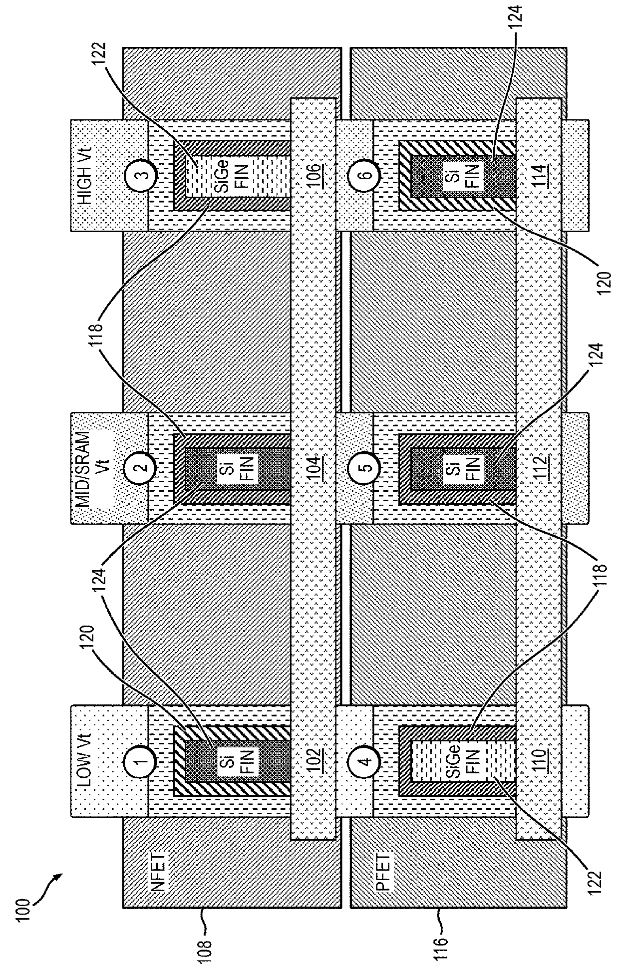
[0024]Principles of the present invention will be described herein in the context of illustrative semiconductor structures and methods for obtaining a plurality of fin-type field-effect transistor (FinFET) devices having different threshold voltages by the novel use and reconfiguration of gate stack material and channel material in the semiconductor structure. It is to be appreciated, however, that the invention is not limited to the specific structures and / or methods illustratively shown and described herein. For example, exemplary FinFET device structures are shown for illustrative purposes, but it is to be appreciated that aspects according to embodiments of the invention can be similarly extended to planar and other non-planar devices as well. Furthermore, illustrative embodiments shown and described herein utilize silicon germanium (SiGe) and silicon (Si) as channel materials but may also be extended to alternative channel materials. Thus, it will become apparent to those skill...


PUM


Abstract

A method of fabricating a semiconductor structure having multiple defined threshold voltages includes: forming multiple field-effect transistor (FET) devices in the semiconductor structure, each of the FET devices including a channel and a gate stack formed of one of at least two different work function metals, the gate stack being formed proximate the channel; and varying a bang-gap of the channel in each of at least a subset of the FET devices by controlling a percentage of one or more compositions of a material forming the channel; wherein a threshold voltage of each of the FET devices is configured as a function of a type of work function metal forming the gate stack and the percentage of one or more compositions of the material forming the channel.

Description

BACKGROUND OF THE INVENTION[0001]The present invention relates generally to the electrical, electronic and computer arts, and, more particularly, to semiconductor structures.[0002]Threshold voltage definition is probably one of the most critical parameters in complementary metal-oxide-semiconductor (CMOS) processing technology since it strongly determines the performance of CMOS devices with a given overdrive. In polysilicon / silicon oxynitride (SiON) technology, the threshold voltage was defined by a combination of well / halo / extension doping along with a doping of the gate. As high dielectric constant, or “high-K,” metal gate technology was introduced, the gate doping knob was eliminated and replaced with the use of discrete work function metals, thus making it more challenging to obtain varying threshold voltages for a multitude of devices in a chip.[0003]As semiconductor device scaling progresses, fully-depleted device technology is surfacing. In a fully-depleted device process te...

Claims


Application Information

Patent Timeline
IPC IPC(8): H01L27/092H01L21/8234H01L21/02H01L29/423H01L21/28H01L29/161H01L29/49H01L27/11H01L29/10
CPCH01L27/0922H01L21/823412H01L21/82345H01L21/02532H01L21/823431H01L29/1033H01L21/28088H01L29/161H01L27/0924H01L29/4966H01L27/1104H01L29/42392H01L21/823807H01L21/823821H01L21/823842H01L27/092H10B10/12
Inventor JAGANNATHAN, HEMANTHNARAYANAN, VIJAY
Owner IBM CORP
Why Eureka
Try Eureka