Zinc oxide nano-ultraviolet light sensor and preparation method thereof
A zinc oxide nanometer and sensor technology, which is applied in the direction of zinc oxide/zinc hydroxide, semiconductor devices, and final product manufacturing, and can solve problems such as the practical application of cumbersome and complicated processes
- Summary
- Abstract
- Description
- Claims
- Application Information
AI Technical Summary
Problems solved by technology
Method used
Image

Examples
Embodiment 1
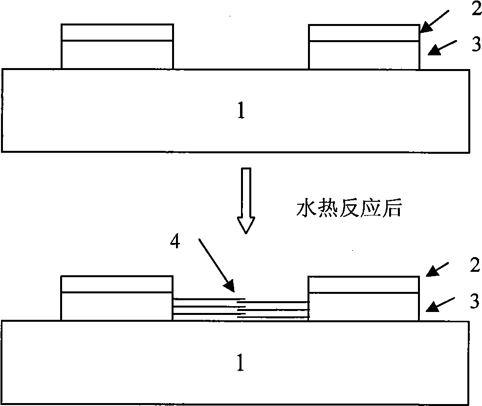
[0025] See attached figure 2 , in this example, ordinary glass is used as the substrate, and a traditional photolithography mask is used as an example to illustrate. Specific steps are as follows:
[0026] 1. Use traditional semiconductor technology to clean ordinary blank glass substrates.
[0027] 2. Make a layer of photoresist mask on the glass substrate using traditional photolithography technology.
[0028] 3. Deposit a layer of 300nm ZnO thin film on the glass substrate as the seed layer.
[0029] 4. Deposit a layer of 50nm Sn film on the substrate as a passivation layer and also as an electrode.
[0030] 5. Use the traditional photoresist removal method to wash off the photoresist to obtain the required interdigitated electrodes.
[0031] 6. A high-pressure hydrothermal reactor with polytetrafluoroethylene lining is used as the reaction vessel, and the aqueous solution is zinc acetate and hexamethylene tetramine with a concentration of 0.005mol / L. Put the sample f...
Embodiment 2
[0035] See attached image 3 , in this example, silicon dioxide is used as the substrate, and a traditional photolithography mask is used as an example to illustrate.
[0036] Specific steps are as follows:
[0037] 1. Clean the silicon dioxide substrate using traditional semiconductor processes.
[0038] 2. Make a layer of photoresist mask on the silicon dioxide substrate using traditional photolithography technology.
[0039]3. Deposit a layer of 200nm aluminum-doped zinc oxide film on the silicon dioxide substrate as a seed layer.
[0040] 4. Deposit a layer of 50nm Cr thin film on the silicon dioxide substrate as a passivation layer, and also as an electrode.
[0041] 5. Use the traditional photoresist removal method to wash off the photoresist to obtain the required interdigitated electrodes.
[0042] 6. A high-pressure hydrothermal reactor lined with polytetrafluoroethylene is used as the reaction vessel, and the aqueous solution is zinc acetate and hexamethylene tet...
Embodiment 3
[0046] See attached Figure 4 , In this example, the flexible substrate PET (polyethylene terephthalate) is used as the substrate, and the metal mask is used as an example to illustrate. Specific steps are as follows:
[0047] 1. Clean the PET flexible substrate with absolute ethanol and deionized water and dry it for use.
[0048] 2. Using a metal mask as a mask, deposit a 30nm gold thin film on the substrate as a seed layer.
[0049] 3. Deposit a layer of 50nm ITO film on the substrate as a passivation layer and also as an electrode.
[0050] 4. A high-pressure hydrothermal reactor with polytetrafluoroethylene lining is used as the reaction vessel, and the aqueous solution is zinc acetate and hexamethylene tetramine with a concentration of 0.001mol / L. Put the sample face down and place it horizontally below the liquid level in the reaction kettle, put the autoclave in a constant temperature box, and keep it at 65°C for three hours.
[0051] 5. Take out the sample, rinse ...
PUM
 Abstract
Description
Claims
Application Information
 - R&D Engineer
- R&D Manager
- IP Professional
- Industry Leading Data Capabilities
- Powerful AI technology
- Patent DNA Extraction
Browse by: Latest US Patents, China's latest patents, Technical Efficacy Thesaurus, Application Domain, Technology Topic.
© 2024 PatSnap. All rights reserved.Legal|Privacy policy|Modern Slavery Act Transparency Statement|Sitemap