Packaging structure and method of photoelectronic device

A technology of optoelectronic devices and packaging structures, applied in the field of optoelectronics, can solve problems such as device performance degradation, stability degradation, and material deterioration, and achieve the effects of prolonging device life, simplifying processes, and reducing costs

Inactive Publication Date: 2015-09-23
UNIV OF ELECTRONICS SCI & TECH OF CHINA
View PDF4 Cites 0 Cited by
  • Summary
  • Abstract
  • Description
  • Claims
  • Application Information

AI Technical Summary

Problems solved by technology

The oxygen content in the atmosphere oxidizes organic materials and generates carbonyl compounds. This compound is a serious quencher and will cause material deterioration. Material deterioration will form black spots, accompanied by device performance degradation
The influence of moisture is more obvious, and its main damage mode is the hydrolysis of the organic layer compound by the conductive electrode, which greatly reduces the stability

Method used


Image

  • Packaging structure and method of photoelectronic device
  • Packaging structure and method of photoelectronic device
  • Packaging structure and method of photoelectronic device

Examples


Embodiment 1

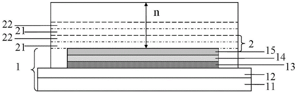
[0035] Such as figure 1 As shown, 1 is an organic electroluminescent device, the anode layer 12 is ITO, and the hole transport layer 13 is N,N'-bis(naphthylidene-1-yl)-N,N'-bis(phenyl) - benzidine (NPB), electron transport layer 14 is 1,3,5-(triN-phenyl-2-benzimidazole-2) benzene 41 (TPBi), cathode layer 15 is Mg:Ag alloy, inorganic package Material layer 21 is Al 2 o 3 , the UV-curable resin layer 22 includes 70% shellac, 18% reactive diluent and 12% triaryl sulfur type hexafluorophosphonium salt, the number of cycles n is 24, and the device structure is:

[0036] Glass substrate / ITO / NPB(50nm) / TPBi(30nm) / Mg:Ag(200nm) / [Al 2 o 3 (200nm) / UV curable resin (100nm)] 24

[0037] The preparation method is as follows:

[0038] ①Use detergent, acetone solution, ethanol solution and deionized water to ultrasonically clean the substrate and dry it with nitrogen;

[0039] ②Transfer the clean substrate to the high vacuum evaporation chamber, and keep the pressure of the organic cav...

Embodiment 2

[0047] Such as figure 1 As shown, 1 is an organic electroluminescent device, the anode layer 12 is ITO, and the hole transport layer 13 is N,N'-bis(naphthylidene-1-yl)-N,N'-bis(phenyl) - benzidine (NPB), electron transport layer 14 is 1,3,5-(triN-phenyl-2-benzimidazole-2) benzene 41 (TPBi), cathode layer 15 is Mg:Ag alloy, inorganic package Material layer 21 is Al 2 o 3 , the UV-curable resin layer 22 includes 71% shellac, 17% reactive diluent and 12% triaryl sulfur type hexafluorophosphonium salt, the number of cycles n is 20, and the device structure is:

[0048] Glass substrate / ITO / NPB(50nm) / TPBi(30nm) / Mg:Ag(200nm) / [Al 2 o 3 (200nm) / UV curable resin (100nm)] 20

[0049] The preparation method is similar to Example 1.

Embodiment 3

[0051] Such as figure 1 As shown, 1 is an organic electroluminescent device, the anode layer 12 is ITO, and the hole transport layer 13 is N,N'-bis(naphthylidene-1-yl)-N,N'-bis(phenyl) - benzidine (NPB), electron transport layer 14 is 1,3,5-(triN-phenyl-2-benzimidazole-2) benzene 41 (TPBi), cathode layer 15 is Mg:Ag alloy, inorganic package Material layer 21 is Al 2 o 3 , the UV-curable resin layer 22 includes 71% shellac, 18% reactive diluent and 11% triaryl sulfur type hexafluorophosphonium salt, the number of cycles n is 16, and the device structure is:

[0052] Glass substrate / ITO / NPB(50nm) / TPBi(30nm) / Mg:Ag(200nm) / [Al 2 o 3 (200nm) / UV curable resin (100nm)] 16

[0053] The preparation method is similar to Example 1.


PUM


Abstract

The invention discloses a packaging structure and method of a photoelectronic device. The photoelectronic device is packaged in a film packaging method, a film packaging layer wraps the photoelectronic device, and formed by laminating inorganic packaging material layers and ultraviolet light solidification resin layers alternatively, and the ultraviolet light solidification resin layers are composed of shellac, a reaction diluents and triaryl sulfur hexafluoride phosphor salt. The packaging method can effectively block oxygen and water in the surrounding, improves the stability of the device, and prolongs the service life of the device; and at the same time, the packaging method is characterized by simple preparation technology and low cost.

Description

technical field [0001] The invention relates to the field of optoelectronic technology, in particular to a packaging structure and a packaging method of an optoelectronic device. Background technique [0002] Today, with the rapid development of electronic technology, optoelectronic technology is one of the rapidly developing high-tech industries after microelectronic technology. With the rapid development of optoelectronic technology, optoelectronic products such as light-emitting diodes, organic light-emitting diodes, solar cells, and thin-film transistors have gradually matured, greatly improving and improving people's lives. At the same time, due to the huge growing market created by the wide application of optoelectronic information technology in various fields of social life, the competition in the field of optoelectronic information is rapidly expanding around the world. [0003] The most widely used optoelectronic devices include organic electroluminescent devices, ...

Claims


Application Information

Patent Timeline
Patent Type & Authority Applications(China)
IPC IPC(8): H01L51/52H01L51/44H01L51/10
CPCH10K10/88H10K30/88H10K50/8445H10K2102/00Y02E10/549
Inventor 于军胜王煦周殿力王晓
Owner UNIV OF ELECTRONICS SCI & TECH OF CHINA
Why Eureka
Try Eureka