Packaging structure and packaging method of optoelectronic device

An optoelectronic device and packaging method technology, applied in the field of optoelectronics, can solve the problems of device performance degradation, material negative effects, device performance degradation, etc., to achieve the effects of optimizing device performance, improving barrier function, and prolonging device life.

Inactive Publication Date: 2015-09-02
UNIV OF ELECTRONIC SCI & TECH OF CHINA
View PDF8 Cites 3 Cited by
  • Summary
  • Abstract
  • Description
  • Claims
  • Application Information

AI Technical Summary

Problems solved by technology

Although organic optoelectronic devices have excellent performance, there are still some problems to be solved: since most of their components are made of organic materials on rigid (such as glass or silicon wafer) or flexible substrates, and the organic materials themselves are harmful to the external environment. Strong sensitivity, as time goes by, the water and oxygen in the atmospheric environment will have a serious negative effect on the material, so that the performance of the unpackaged device will gradually decrease after being placed in the atmospheric environment, or even completely lose performance
Specifically, oxygen oxidizes organic materials to generate carbonyl compounds, which are serious quenchers. In addition, material deterioration will form black spots, accompanied by device performance degradation
The influence of water vapor is more obvious, and its main damage method is the hydrolysis of the organic layer compound by the conductive electrode, which greatly reduces the stability

Method used


Image

  • Packaging structure and packaging method of optoelectronic device
  • Packaging structure and packaging method of optoelectronic device
  • Packaging structure and packaging method of optoelectronic device

Examples


Embodiment 1

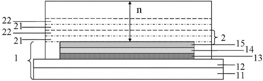
[0030] Such as figure 1 As shown, 1 is an organic electroluminescent device, the anode layer 12 is ITO, and the hole transport layer 13 is N,N'-bis(naphthylidene-1-yl)-N,N'-bis(phenyl) - benzidine (NPB), electron transport layer 14 is 1,3,5-(triN-phenyl-2-benzimidazole-2) benzene 41 (TPBi), cathode layer 15 is Mg:Ag alloy, inorganic package Material layer 21 is Al 2 o 3 , the UV curable resin layer 22 includes 58% shellac, 3% glycerin, 0.97% lead oxide, 4% toluene diisocyanate, 9% trimethylol propane, 0.01% hydroquinone, 11% tetrahydrofuran, 7% 2-hydroxyethyl methacrylate, 0.02% dibutyltin dilaurate, 2% 2,2-dimethoxy-phenyl ketone and 5% trimethylol Propane triacrylate, the period number n is 20, and the device structure is:

[0031] Glass substrate / ITO / NPB(50nm) / TPBi(30nm) / Mg:Ag(200nm) / [Al 2 o 3 (200nm) / UV curable resin (100nm)] 20

[0032] The preparation method is as follows:

[0033] ①Use detergent, acetone solution, ethanol solution and deionized water to ultraso...

Embodiment 2

[0042] Such as figure 1 As shown, 1 is an organic electroluminescent device, the anode layer 12 is ITO, and the hole transport layer 13 is N,N'-bis(naphthylidene-1-yl)-N,N'-bis(phenyl) - benzidine (NPB), electron transport layer 14 is 1,3,5-(triN-phenyl-2-benzimidazole-2) benzene 41 (TPBi), cathode layer 15 is Mg:Ag alloy, inorganic package Material layer 21 is Al 2 o 3 , the UV curable resin layer 22 includes 53% shellac, 5% glycerin, 0.005% lead oxide, 4% toluene diisocyanate, 9% trimethylol propane, 0.005% hydroquinone, 12% tetrahydrofuran, 7% 2-hydroxyethyl methacrylate, 0.99% dibutyltin dilaurate, 3% 2,2-dimethoxy-phenyl ketone and 6% trimethylol Propane triacrylate, the period number n is 16, and the device structure is:

[0043] Glass substrate / ITO / NPB(50nm) / TPBi(30nm) / Mg:Ag(200nm) / [Al 2 o 3 (200nm) / UV curable resin (100nm)] 16

[0044] The preparation method is similar to Example 1.

Embodiment 3

[0046] Such as figure 1 As shown, 1 is an organic electroluminescent device, the anode layer 12 is ITO, and the hole transport layer 13 is N,N'-bis(naphthylidene-1-yl)-N,N'-bis(phenyl) - benzidine (NPB), electron transport layer 14 is 1,3,5-(triN-phenyl-2-benzimidazole-2) benzene 41 (TPBi), cathode layer 15 is Mg:Ag alloy, inorganic package Material layer 21 is Al 2 o 3 , the UV curable resin layer 22 includes 39% shellac, 5% glycerol, 0.003% lead oxide, 7% toluene diisocyanate, 10% trimethylol propane, 0.097% hydroquinone, 10% tetrahydrofuran, 7.9% 2-hydroxyethyl methacrylate, 1% dibutyltin dilaurate, 9% 2,2-dimethoxy-phenyl ketone and 11% trimethylol Propane triacrylate, the period number n is 12, and the device structure is:

[0047] Glass substrate / ITO / NPB(50nm) / TPBi(30nm) / Mg:Ag(200nm) / [Al 2 o 3 (200nm) / UV curable resin (100nm)] 12

[0048] The preparation method is similar to Example 1.


PUM


Abstract

The invention discloses a packaging structure and a packaging method of an optoelectronic device. The packaging structure of the optoelectronic device includes a thin film packaging layer used for wrapping the optoelectronic device, and is characterized in that the thin film packaging layer is formed by alternately overlapping inorganic packaging material layers and ultraviolet curing resin layers with a period number n, wherein 1<=n<=20, ultraviolet curing resin comprises the following components by mass percent: lac, glycerol, lead oxide, toluene diisocynate, trimethylolpropane, hydroquinone, tetrahydrofuran, 2-hydroxyethyl methyl acrylate, dibutyltin dilaurate, 2,2-dimethoxy-phenyl ketone and trimethylolpropane triacrylate. The packaging structure can effectively block oxygen and water in ambient environment, thereby facilitating improvement of stability of the device and prolonging of the life of the device; and at the same time, the packaging method has the characteristics of simple preparation technology and low cost.

Description

technical field [0001] The invention relates to the field of optoelectronic technology, in particular to a packaging structure and a packaging method of an optoelectronic device. Background technique [0002] In the past 10 years, with the rapid development of optoelectronic technology, optoelectronic products such as light-emitting diodes, organic light-emitting diodes, solar cells, and thin-film transistors have gradually matured, greatly improving people's lives, and becoming the most promising high-tech industry. At the same time, the wide application of optoelectronic information technology in various fields of social life has also created a huge growing market. The competition in the field of optoelectronic information is unfolding worldwide, and it will surely become the most active research direction in the field of electronic information in the future. [0003] Optoelectronic devices mainly include organic electroluminescent devices, inorganic light-emitting diodes,...

Claims


Application Information

Patent Timeline
IPC IPC(8): H01L33/56H01L51/52
CPCH01L33/56H01L2933/005H10K50/8426
Inventor 于军胜王煦范惠东王瀚雨
Owner UNIV OF ELECTRONIC SCI & TECH OF CHINA
Why Eureka
Try Eureka