
Special fixture for manufacturing process of semiconductor module and sliding block component thereof

A manufacturing process and special fixture technology, applied in semiconductor/solid-state device manufacturing, electrical components, circuits, etc., can solve problems such as increased manufacturing costs, easy drop of workpieces, and poor return function of steel springs

Inactive Publication Date: 2009-10-07
SAMSUNG ELECTRONICS SUZHOU SEMICON
View PDF0 Cites 10 Cited by
  • Summary
  • Abstract
  • Description
  • Claims
  • Application Information

AI Technical Summary

Problems solved by technology

The frictional force causes the return function of the steel spring to deteriorate, so that the workpiece cannot be firmly fixed, which makes the workpiece easy to fall during actual work, resulting in an increase in manufacturing costs
And, since the other end of the steel spring is fixed on the fixture through the groove (that is, the steel spring groove), the steel spring groove will be worn when repairing the damaged steel spring or slider, which causes the slider corresponding to the steel spring to wear. Block-fixed workpieces cannot be positioned well and eventually the entire fixture is scrapped

Method used


Image

  • Special fixture for manufacturing process of semiconductor module and sliding block component thereof
  • Special fixture for manufacturing process of semiconductor module and sliding block component thereof
  • Special fixture for manufacturing process of semiconductor module and sliding block component thereof

Examples


Embodiment Construction

[0016] Hereinafter, embodiments of the present invention will be described in detail with reference to the drawings.

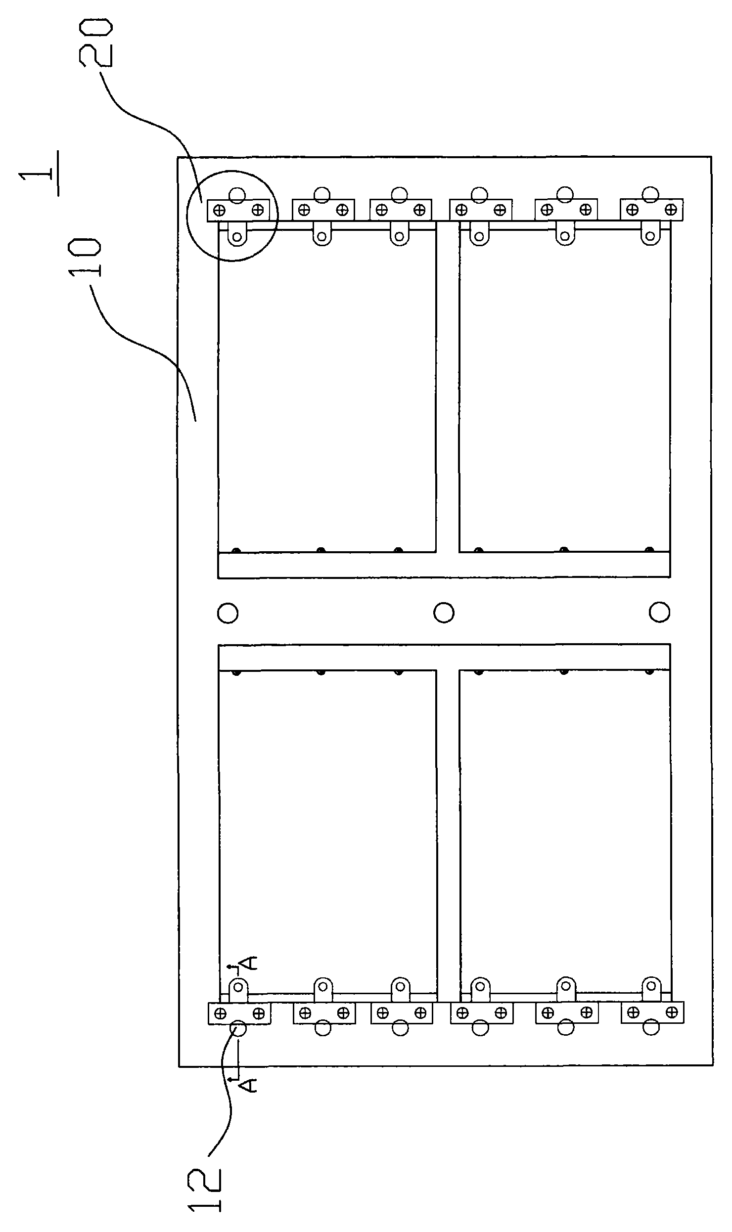
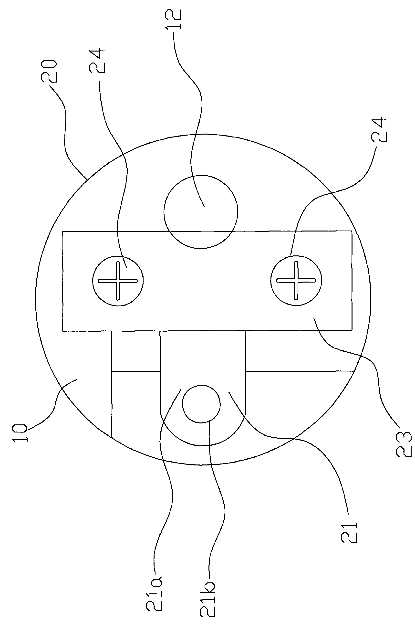
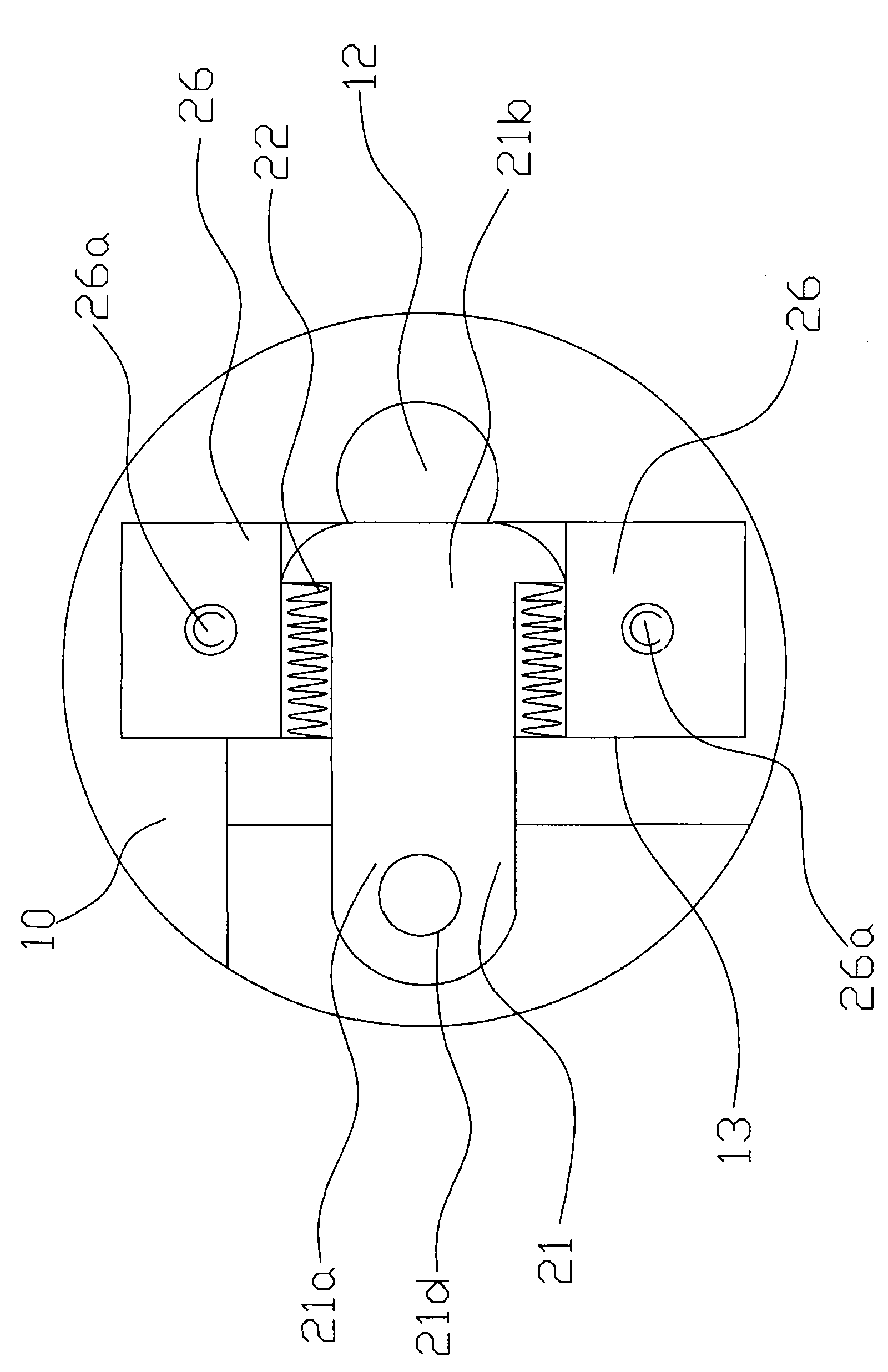
[0017] figure 1 is a plan view showing a jig 1 dedicated to a semiconductor module manufacturing process according to an exemplary embodiment of the present invention. figure 2 is a partial plan view showing the structure of a positioning slider according to an exemplary embodiment of the present invention. image 3 is a partial top view showing the structure of the positioning slider after the cover sheet and screws are removed according to an exemplary embodiment of the present invention.

[0018] like figure 1 As shown, the jig 1 includes a jig body 10 with a certain thickness and several slider assemblies 20 . On the fixture main body 10, there are: several positioning protrusions 11 for matching with positioning holes (not shown) of the workpiece; several thimble holes 12 formed through the fixture main body 10 for making the loading tool (not shown) ...


PUM


Abstract

The invention discloses a special fixture for the manufacturing process of a semiconductor module. The fixture comprises a main body and a sliding block component; the main body of the fixture is provided with a plurality of sliding grooves, a plurality of center holes and a plurality of positioning bulges; one side of the sliding groove is provided with a notch, and the notch is externally communicated; and the sliding block component is arranged in the corresponding sliding grooves. The fixture is characterized in that: the sliding block component comprises sliding blocks, an elastic component and a cover plate, wherein the sliding blocks slide in the corresponding sliding grooves, and one end of the sliding block extends from the notch of the sliding groove; the elastic component is arranged along the sliding direction of the sliding blocks, one end thereof is supported by the other end opposite to the above end of the sliding block, while the other end thereof is supported by the side wall at the side with the notch of the sliding groove, and the elastic component is used for driving the sliding grooves to slide toward the corresponding center holes through the restoring force thereof; and the cover plate is used for covering the sliding blocks and the elastic component so as to prevent the sliding blocks and the elastic component from deviating from the sliding grooves. The fixture utilizes the direct motion of the built-in elastic component, has good resetting property of the sliding blocks thereof, and uses the cover plate for covering the sliding blocks and the elastic component, thus facilitating the maintenance.

Description

technical field [0001] The present invention relates to a special jig for fixing semiconductor modules during semiconductor manufacturing or testing. Background technique [0002] During the semiconductor manufacturing process, for example, during the high-precision surface mount process, it is necessary to fix the semiconductor module on a dedicated jig to perform various manufacturing processes. In addition, after the production process of the semiconductor module is completed, it is generally necessary to conduct an appearance inspection on the product to determine whether the product has obvious defects. Due to the high manufacturing precision and high integration of semiconductor products, it is easy to damage the products during the operation and processing of semiconductor products, thereby increasing the scrap rate and increasing the manufacturing cost. [0003] Whether it is in the production process or the inspection process, in order to improve production efficie...

Claims


Application Information

Patent Timeline
IPC IPC(8): H01L21/687H01L21/68
Inventor 汪胜琴郭士达
Owner SAMSUNG ELECTRONICS SUZHOU SEMICON
Learn More