Semiconductor device, manufacturing method for semiconductor device, and electronic equipment

Inactive Publication Date: 2007-01-11
SEIKO EPSON CORP
View PDF10 Cites 87 Cited by
  • Summary
  • Abstract
  • Description
  • Claims
  • Application Information

AI Technical Summary

Benefits of technology

[0043] According to this configuration, a semiconductor device in which detachment of sealing resin

Problems solved by technology

This has been accompanied by the problem of achieving higher semiconductor chip packaging densities, as t

Method used


Image

  • Semiconductor device, manufacturing method for semiconductor device, and electronic equipment
  • Semiconductor device, manufacturing method for semiconductor device, and electronic equipment
  • Semiconductor device, manufacturing method for semiconductor device, and electronic equipment

Examples


first embodiment

[0055] First, the semiconductor device of a first embodiment of the invention is explained, referring to FIG. 1 and FIG. 2A.

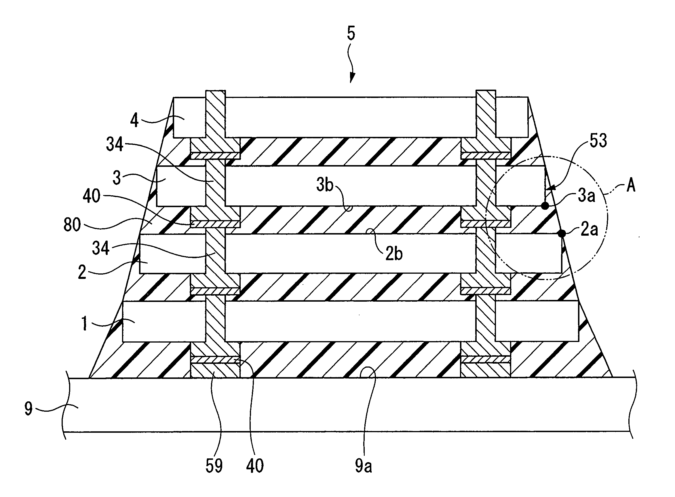
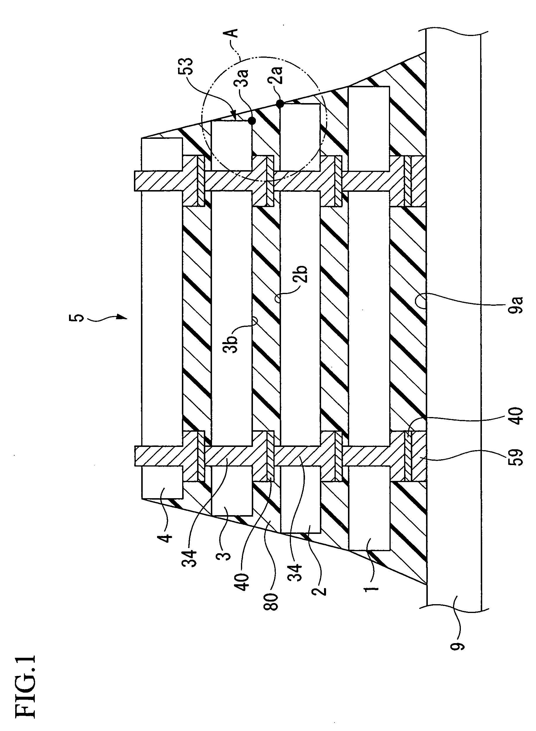
[0056]FIG. 1 is a cross-sectional view of the semiconductor device of the first embodiment.

[0057] The semiconductor device 5 of the first embodiment includes a plurality of stacked semiconductor chips 1, 2, 3, and 4.

[0058] The plurality of semiconductor chips 1, 2, 3, and 4 are positioned on the packaging surface 9a of a circuit substrate 9 (substrate).

[0059] The external sizes of the plurality of semiconductor chips 1, 2, 3, and 4 become successively smaller in moving from the packaging surface 9a of the circuit substrate 9 in the perpendicular direction.

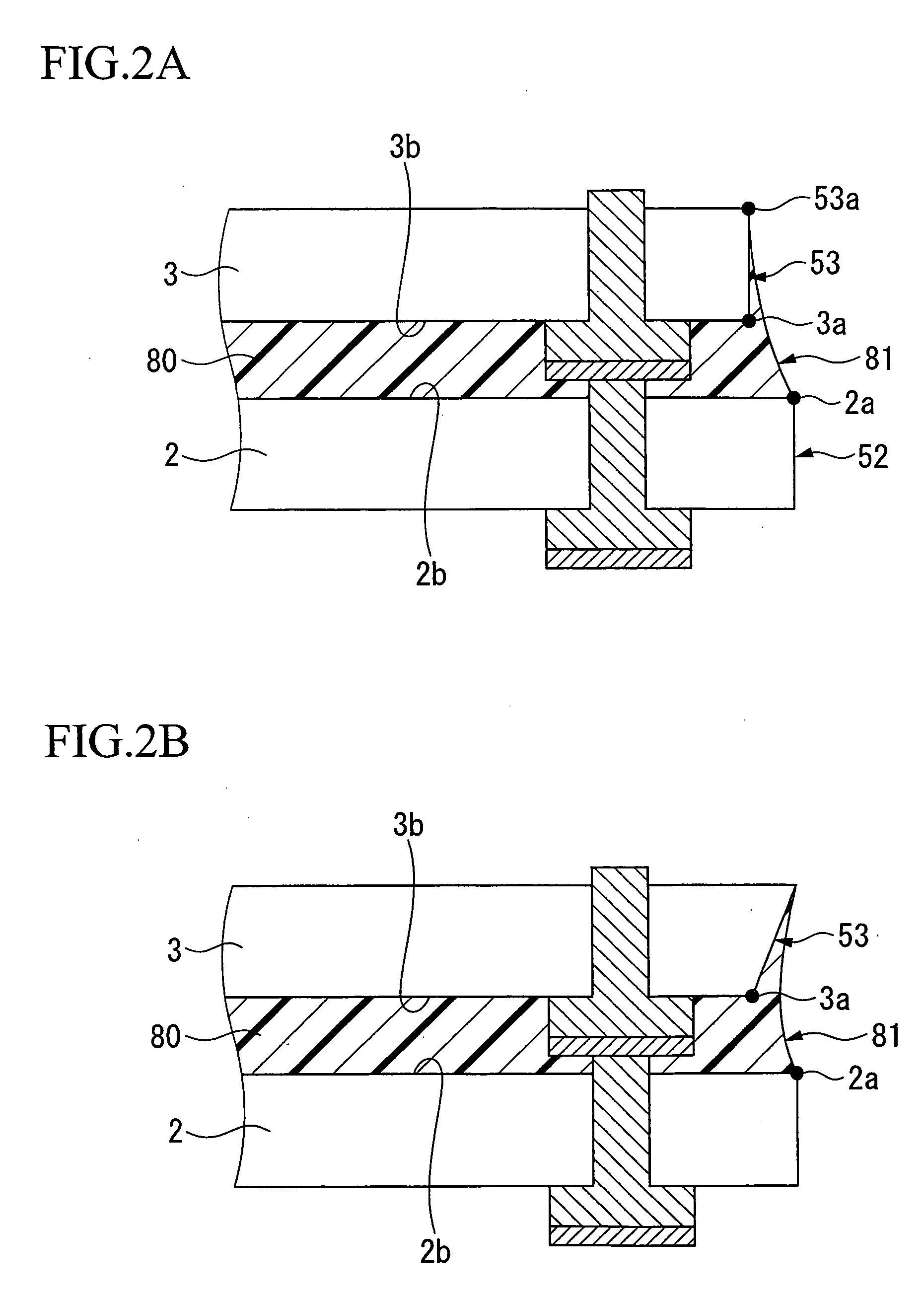
[0060] As shown in FIG. 1, the upper-side semiconductor chip 3 (first semiconductor chip) having a first surface 3b and the lower-side semiconductor chip 2 (second semiconductor chip) having a second surface 2b are mutually faced.

[0061] Here, the first surface 3b of the upper-side semiconductor chip 3 is...

second embodiment

[0129] Next, the semiconductor device of a second embodiment of the invention is explained, referring to FIG. 2B.

[0130]FIG. 2B is a cross-sectional view of the semiconductor device of the second embodiment.

[0131] In the second embodiment, the size of the upper-side semiconductor chip 3 is equal to that of the lower-side semiconductor chip 2, but an inclined surface is formed on the side surface 53 of the upper-side semiconductor chip 3.

[0132] This inclined surface can be formed by anisotropic etching of the silicon substrate.

[0133] By forming this inclined surface, the peripheral portion 3a of the first surface 3b of the upper-side semiconductor chip 3 is positioned on the inner side of the peripheral portion 2a of the second surface 2b of the lower-side semiconductor chip 2.

[0134] Even when liquid sealing resin 80 is filled into the spaces between these semiconductor chips 2 and 3, the end portion 81 of the sealing resin 80 wets the side surface 53 of the upper-side semiconduc...

third embodiment

[0137] Next, the semiconductor device of a third embodiment of the invention is explained, referring to FIG. 3A.

[0138]FIG. 3A is a cross-sectional view of the semiconductor device of the third embodiment.

[0139] In the third embodiment also, the size of the upper-side semiconductor chip 3 is equal to that of the lower-side semiconductor chip 2.

[0140] However, in the third embodiment, a chamfer portion 55 is formed in the peripheral portion 3a of the first surface 3b of the upper-side semiconductor chip 3, as shown in FIG. 3A.

[0141] By this means, the peripheral portion 3a of the first surface 3b of the upper-side semiconductor chip 3 is positioned on the inner side of the peripheral portion 2a of the second surface 2b of the lower-side semiconductor chip 2.

[0142] When liquid sealing resin 80 is filled into the space between the semiconductor chips 2 and 3, the end portion 81 of the sealing resin 80 wets the side surface 53 of the upper-side semiconductor chip 3 up to the upper e...


PUM


Abstract

A semiconductor device includes: a plurality of stacked semiconductor chips including a first semiconductor chip having a side surface, and a second semiconductor chip stacked on the first semiconductor chip; and a sealing resin placed between the plurality of semiconductor chips, at least one edge of the first semiconductor chip is positioned on an inner side of the second semiconductor chip, and the sealing resin placed between the first semiconductor chip and the second semiconductor chip is extended over the side surface of the first semiconductor chip.

Description

CROSS-REFERENCE TO RELATED APPLICATION [0001] This application claims priority from Japanese Patent Application No. 2005-184651, filed Jun. 24, 2005, and Japanese Patent Application No. 2006-059963, filed Mar. 6, 2006, the contents of which are incorporated herein by reference. BACKGROUND [0002] 1. Technical Field [0003] This invention relates to a semiconductor device, a manufacturing method for a semiconductor device, and an electronic equipment. [0004] 2. Related Art [0005] Portable telephone sets, notebook-type personal computers, PDAs (Personal Data Assistants), and other portable electronic equipment are required to be compact and lightweight. [0006] This has been accompanied by the problem of achieving higher semiconductor chip packaging densities, as the packaging space for semiconductor chips in portable electronic equipment has become extremely limited. [0007] As a result, there have been proposals of three-dimensional packaging technologies for semiconductor chips. [0008]...

Claims


Application Information

Patent Timeline
IPC IPC(8): H01L23/02H01L21/00
CPCH01L23/481H01L25/0657H01L2224/16145H01L2224/32145H01L2225/06513H01L2225/06517H01L2924/04941H01L2225/06555H01L2225/06582H01L2225/06596H01L2924/01078H01L2924/01079H01L2225/06541H01L2224/05011H01L2224/05009H01L2224/05548H01L2224/13025H01L2224/05023H01L2224/05124H01L2224/05147H01L2224/05647H01L2224/05684H01L2224/05166H01L2224/02372H01L24/05H01L2924/00014H01L23/12H01L25/065
Inventor FUKAZAWA, MOTOHIKO
Owner SEIKO EPSON CORP
Why Eureka
Try Eureka