

Method for improving imaging properties of an optical system, and optical system
A technology of optical system and imaging characteristics, used in optics, microlithography exposure equipment, optomechanical equipment, etc., to achieve the effect of large deformation and reduced maintenance time
- Summary
- Abstract
- Description
- Claims
- Application Information
AI Technical Summary
Problems solved by technology
Method used
Image

Examples
Embodiment Construction
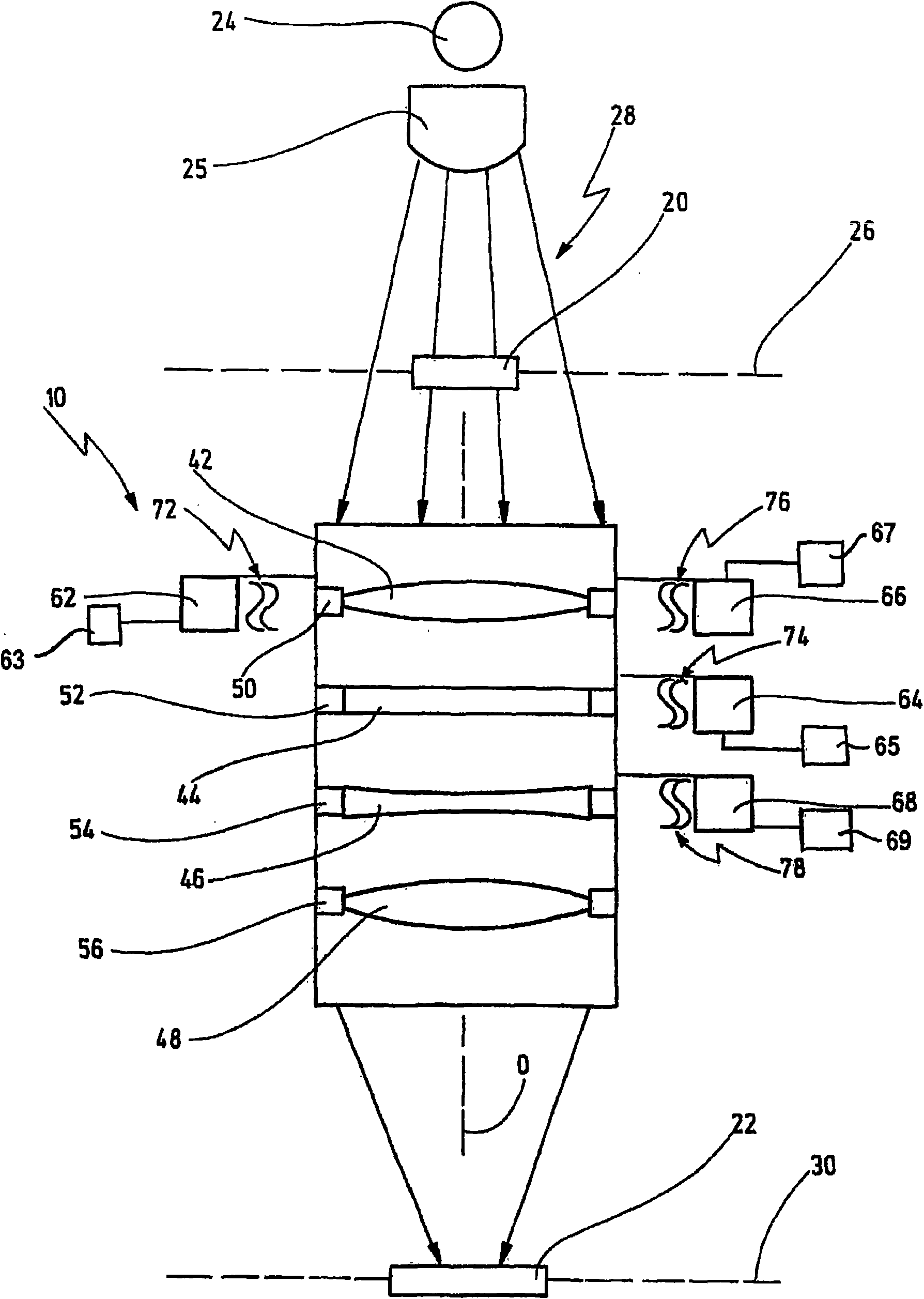
[0083] figure 1 An optical system is shown, which is given the general reference 10 and which allows imaging of a pattern of a structure 20 or mask (reticle) onto a photosensitive substrate 22 .
[0084]An optical system 10 of this type can be used as a projection objective for fabricating finely patterned features in microlithography.
[0085] A light source 24 to which an illumination optics assembly 25 is assigned illuminates a structure 20 disposed in an object plane 26 of the optical system 10 . A light beam 28 is transmitted through a partial area of the structure 20 and into the optical system 10 . The optical system 10 images the structure 20 in a reduced manner onto the photosensitive substrate 22 which is placed in the image plane 30 of the optical system 10 .
[0086] The optical system 10 has a plurality of optical elements, in the schematic illustration, four optical elements 42-48, which may be formed as lenses, mirrors, or parallel plane plates with various ...
PUM
 Abstract
Description
Claims
Application Information