
Organic light emitting diode display device and manufacturing method thereof

一种发光二极管、显示装置的技术,应用在半导体/固态器件制造、晶体管、电气元件等方向,能够解决显示装置亮度不稳定等问题,达到亮度稳定、减小漏电流的效果

Active Publication Date: 2011-12-07
INNOCOM TECH (SHENZHEN) CO LTD +1
View PDF0 Cites 1 Cited by
  • Summary
  • Abstract
  • Description
  • Claims
  • Application Information

AI Technical Summary

Problems solved by technology

[0008] In order to solve the problem of unstable brightness of organic light emitting diode display devices in the prior art, it is necessary to provide an organic light emitting diode display device with stable brightness

Method used


Image

  • Organic light emitting diode display device and manufacturing method thereof
  • Organic light emitting diode display device and manufacturing method thereof
  • Organic light emitting diode display device and manufacturing method thereof

Examples


Embodiment Construction

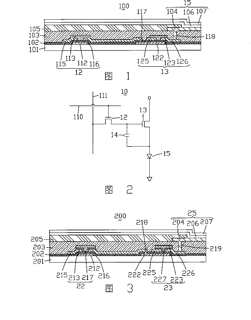
[0028] see image 3 , image 3 It is a schematic cross-sectional view of the organic light emitting diode display device 200 of the present invention. The organic light emitting diode display device 200 includes a substrate 201, a first grid 212 and a second grid 222 located on the substrate 201, a dielectric insulation covering the first grid 212 and the second grid 222 Layer 202, a first source 215, a first drain 216, a second source 225, and a second drain 226 on the dielectric insulating layer 202, a first source 215 and a first drain 216 on the first doped layer 217, a second doped layer 227 on the second source 225 and the second drain 226, a first active layer 213 on the first doped layer 217, A second active layer 223 on the second doped layer 227, a second active layer 223 on the dielectric insulating layer 202, the first source 215 and the first drain 216, the second source 225 and the second drain pole 226 and the passivation layer 203 on the first doped layer 21...


PUM


Abstract

The present invention relates to an organic light emitting diode display device and a manufacturing method thereof. The organic light emitting diode display device includes a plurality of organic thin film transistors, and each organic thin film transistor includes a gate, a dielectric insulating layer on the gate, A channel layer is located on the dielectric insulating layer. The channel layer includes a doping layer, the doping layer includes an organic material and a doping substance, the organic material includes one of pentacene or polytrihexyl-thiadiene pentacycle, and the doping substance includes trioxide One of tungsten or 2,3,5,6-tetrafluoro-7,7',8,8'-tetracyanodimethyl-p-benzoquinone, this organic material reacts with doping substances to generate positive charges to neutralize the remaining Negative charges in the channel layer. The OLED display device has relatively stable brightness.

Description

technical field [0001] The invention relates to an organic light emitting diode display device and a manufacturing method thereof. Background technique [0002] Organic Light Emitting Diode (OLED), due to its advantages of high brightness, fast response, thin and short, full color, wide viewing angle range, no need for LCD backlight and power consumption, so There is a tendency to gradually replace twisted nematic (Twist Nematic, TN) and super twisted nematic (SuperTwist Nematic, STN) liquid crystal display devices, and become a new generation of portable information products, mobile phones, personal digital assistants (Personal Digital Assistant) and notebook computers A commonly used display device. [0003] Thin-film transistors in organic light-emitting diode display devices have a key impact on display quality and have been the focus of research. Generally, an organic thin film transistor has a similar structure to a crystalline silicon thin film transistor (Si-TFT), ...

Claims


Application Information

Patent Timeline
Patent Type & Authority Patents(China)
IPC IPC(8): H01L27/32H01L51/05H01L51/40
CPCH01L51/0036H01L27/3274H01L27/283H01L51/0562H10K19/10H10K59/125H10K85/113H10K10/486
Inventor 王世昌吴宏基
Owner INNOCOM TECH (SHENZHEN) CO LTD
Learn More