Array substrate for capacitive in-cell touch panel and method for driving the same, related display panels, and related display apparatus

Active Publication Date: 2017-09-21
BOE TECH GRP CO LTD +1
View PDF4 Cites 16 Cited by
  • Summary
  • Abstract
  • Description
  • Claims
  • Application Information

AI Technical Summary

Benefits of technology

[0005]The present disclosure provides an array substrate. The Array substrate includes a cathode layer with a novel pattern and a novel signal line layout. By using the structure,

Problems solved by technology

They are also relatively thin and light, and often have a wide viewing angle and short response time.
The parasitic capacitance may slow down the response

Method used


Image

  • Array substrate for capacitive in-cell touch panel and method for driving the same, related display panels, and related display apparatus
  • Array substrate for capacitive in-cell touch panel and method for driving the same, related display panels, and related display apparatus
  • Array substrate for capacitive in-cell touch panel and method for driving the same, related display panels, and related display apparatus

Examples


second embodiment

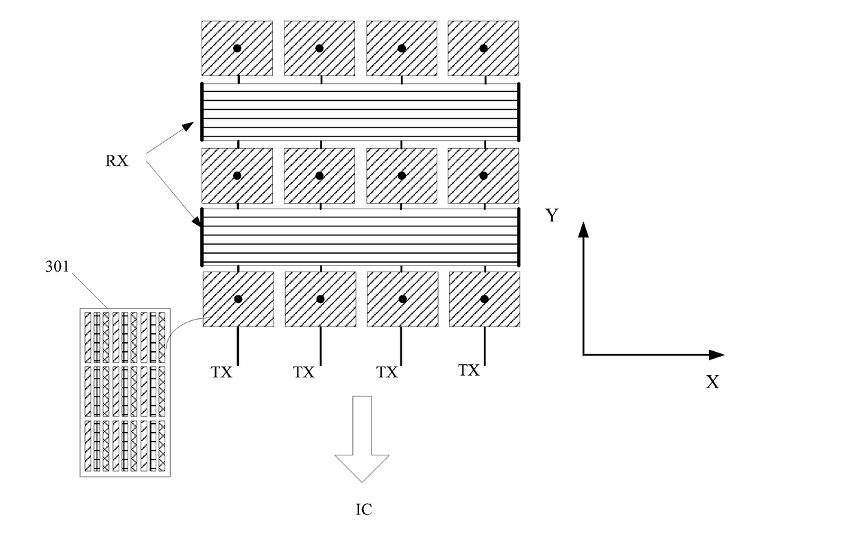
[0067]FIG. 5 illustrates the present disclosure. For viewing simplicity, only the cathode pads, the cathode strips, the cathode voltage lines TXn for the time-sharing operation, and the touch anode voltage lines VDD1 to VDD4 are shown. For illustrative purposes, the normal anode voltage being corresponding to the cathode strips may only represent the normal anode voltage being applied on the anode layers corresponding to the cathode strips. The touch anode voltage lines VDD1 to VDD4 each being corresponding to a column of cathode pads may only represent the touch anode voltages ELVDDn (n=1,2,3,4, etc.) applied by the touch anode voltage line VDDn (n=1, 2, 3, 4, etc.) on the anode layers corresponding to the column of cathode pads. The touch anode voltage ELVDDn (n=1,2,3,4, etc.) may be equal to (ELVDD+Vtouch), i.e., a superimposition of the normal anode voltage ELVDD and the touch driving signal Vtouch. Thus, the touch anode voltage ELVDDn (n=1,2,3,4, etc.) may be a wave-shaped volt...

first embodiment

[0069]Similar to the first embodiment, the operation of the display panel incorporating the cathode layer in FIG. 5 may also include at least a displaying mode and a touch-sensing mode.

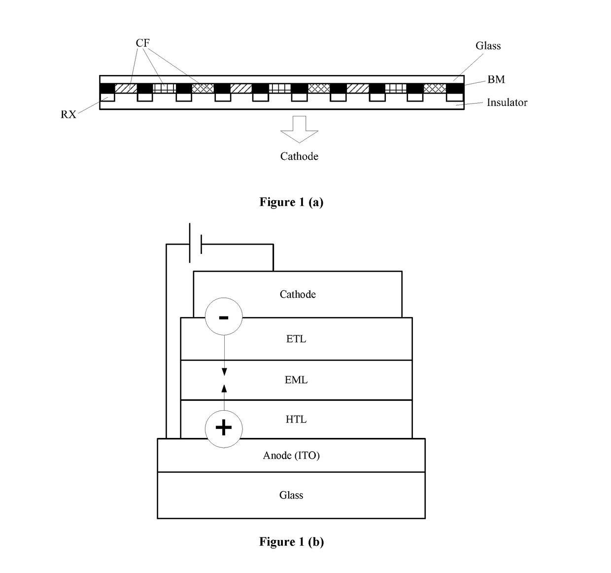
[0070]In the displaying mode and the touch-sensing mode in one frame, a normal cathode voltage may be applied on the cathode strips during the displaying mode and touch-sensing mode by a normal cathode voltage line (not shown in FIG. 5). A normal anode voltage, i.e., a driving voltage, may be applied on the anode layers corresponding to the cathode strips, where the anode layers may refer to the anode layers of the OLEDs corresponding to the cathode strips. During each frame, the cathode voltage (i.e., the normal cathode voltage) and the anode voltage (i.e., the normal anode voltage) applied on the OLEDs corresponding to the cathode strips may be stable, so that the OLEDs may emit light with a stable brightness.

[0071]In the displaying mode of one frame, a normal cathode voltage may be applied on the c...


PUM


Abstract

The present disclosure provides an array substrate for an organic light-emitting diode (OLED) display panel. The array substrate includes a substrate, a thin film transistor (TFT) layer comprising a plurality of TFTs, and an anode layer comprising a plurality of anode electrodes. The array substrate also includes an organic layer comprising a plurality of organic units corresponding to anode electrodes, and a cathode layer comprising a plurality of touch electrodes for a time-sharing operation. Each touch electrode corresponds to a portion of the plurality of organic units, the plurality of the touch electrodes being arranged to be applied with a normal cathode voltage in a displaying period and to be applied with a touch cathode voltage in a touch-sensing period.

Description

FIELD OF THE INVENTION[0001]The present invention generally relates to the display technologies and, more particularly, relates to an array substrate for capacitive in-cell touch panel, a method for driving the array substrate, related display panels, and related display apparatus.BACKGROUND[0002]In an OLED device, the conductive organic layer for emitting light is often positioned between two electrode layers (i.e., the cathode layer and the anode layer) to form a “sandwich” shaped structure. In such an OLED device, holes are injected into the organic layer from the anode and electrons are injected into the organic layer from the cathode. Holes move toward electrons and combine with electrons in the organic layer to form excitons, i.e., a bound state of electron and hole. The decay of the excitons results in relaxation of energy, accompanied by emission of radiation, e.g., visible light. Compared to conventional liquid crystal display (LCD) devices, OLED display devices do not requ...

Claims


Application Information

Patent Timeline
IPC IPC(8): G06F3/041H01L27/32H01L51/52G06F3/044
CPCG06F3/0412G06F3/0416G06F3/044H01L27/3276H01L27/322H01L51/5221H01L27/323G06F2203/04111H10K59/40G06F3/0443G06F3/04164G06F3/04184G06F3/04166H10K50/82H10K59/38H10K59/131G02F1/13338
Inventor DING, XIAOLIANGDONG, XUEWANG, HAISHENGLIU, YINGMINGWANG, LEICHEN, XIAOCHUANREN, TAO
Owner BOE TECH GRP CO LTD
Why Eureka
Try Eureka