Liquid crystal display device and manufacturing method of liquid crystal display device

Active Publication Date: 2012-09-13
SEMICON ENERGY LAB CO LTD
View PDF3 Cites 18 Cited by
  • Summary
  • Abstract
  • Description
  • Claims
  • Application Information

AI Technical Summary

Benefits of technology

[0017]According to one embodiment of the present invention, with the above structure, the thicknesses of a pixel electrode and a common electrode can be larger than those in a vertical electric field mode, and the gradient of a side portion of each of the pixel electrode and the common electrode can be made steep. Further, in the liquid crystal display device having a novel electrode struc

Problems solved by technology

However, it still cannot be said that the consideration of the electrode structure is enough, and it has been desired that a novel electrode structure utilizing characteristics of liquid crystal exhibiting

Method used


Image

  • Liquid crystal display device and manufacturing method of liquid crystal display device
  • Liquid crystal display device and manufacturing method of liquid crystal display device
  • Liquid crystal display device and manufacturing method of liquid crystal display device

Examples


embodiment 1

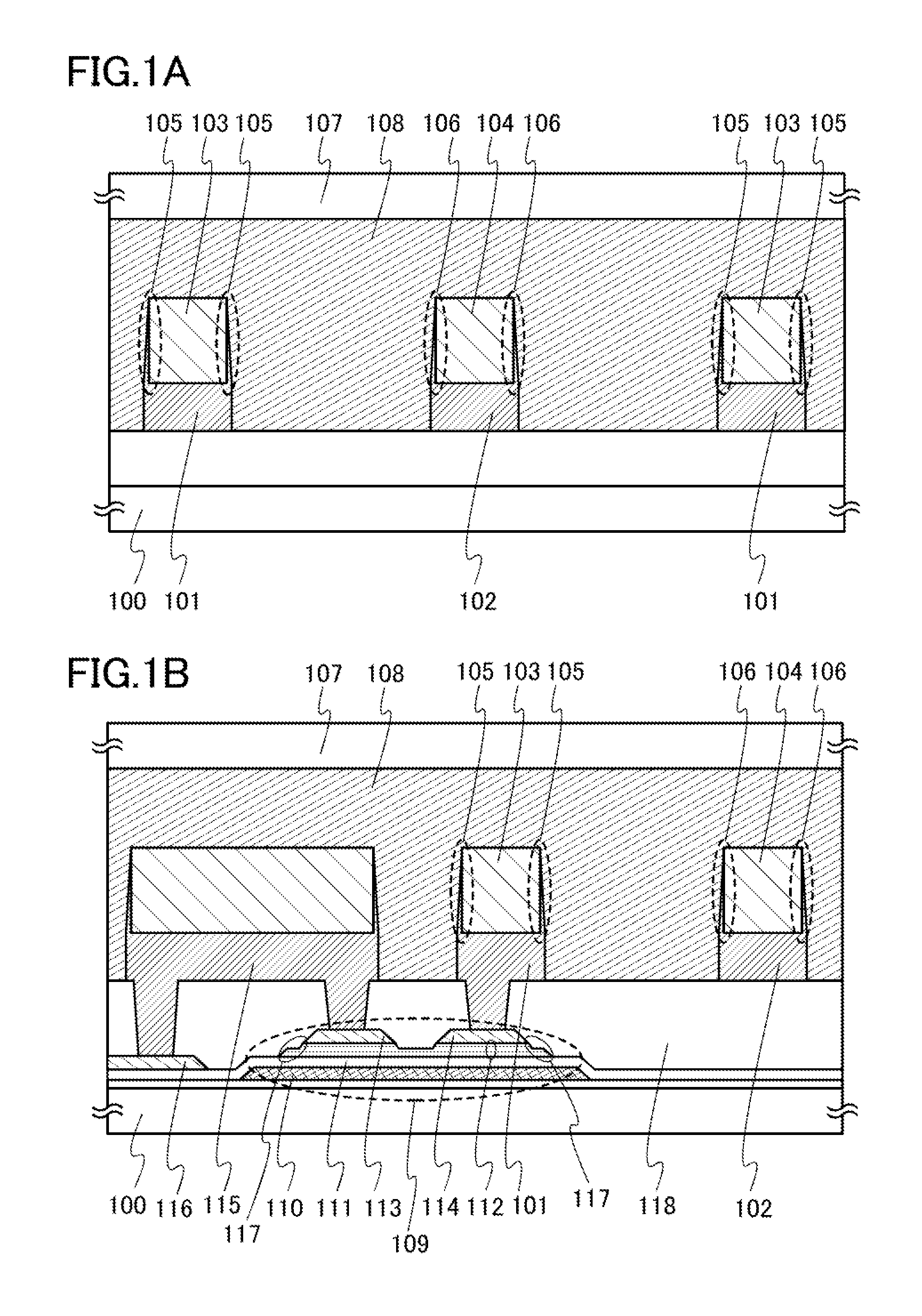
[0035]FIG. 1A illustrates one example of a cross-sectional structure of a pixel electrode and a common electrode in one embodiment of the present invention. In FIG. 1A, a pixel electrode 101 and a common electrode 102 are formed over a substrate 100. Note that a semiconductor element such as a transistor, an insulating film, and a conductive film such as a wiring may be formed between the substrate 100, and the pixel electrode 101 and the common electrode 102.

[0036]An insulating film 103 is formed over the pixel electrode 101, and an insulating film 104 is formed over the common electrode 102. Part of the pixel electrode 101, which is surrounded by a dashed line 105, is positioned on a side portion of the insulating film 103. Similarly, part of the common electrode 102, which is surrounded by a dashed line 106, is positioned on a side portion of the insulating film 104.

[0037]A substrate 107 is provided so as to face the substrate 100 with the pixel electrode 101, the common electrod...

embodiment 2

[0069]In this embodiment, a structure of a pixel of a liquid crystal display device according to one embodiment of the present invention will be described.

[0070]FIG. 3 is an example of a top view of a pixel. FIG. 4 is an enlarged top view of part of the pixel in FIG. 3. FIG. 5 illustrates a cross-sectional view taken along dashed line A1-A2 in FIG. 4, a cross-sectional view taken along dashed line B1-B2 in FIG. 4, and a cross-sectional view taken along dashed line C1-C2 in FIG. 4.

[0071]The pixel in FIG. 3 includes a transistor 301, a pixel electrode 302, a common electrode 303, and a capacitor 304.

[0072]The transistor 301 includes a conductive film 305 functioning as a gate electrode, an active layer 306 formed so as to overlap with the conductive film 305 with an insulating film 320 interposed therebetween, and a conductive film 307 and a conductive film 308 functioning as a source electrode and a drain electrode over the active layer 306.

[0073]The conductive film 305 functions not...

embodiment 3

[0095]In this embodiment, a manufacturing method of the liquid crystal display device illustrated in the cross-sectional views of FIG. 5 according to one embodiment of the present invention will be described with reference to FIGS. 7A to 7D and FIGS. 8A to 8C. Note that in this embodiment, the case where the transistor 301 is an n-channel transistor is given as an example.

[0096]First, the insulating film 319 is formed over the substrate 318, and then, the conductive films 305 and 316 are formed over the insulating film 319 as illustrated in FIG. 7A.

[0097]Although there is no particular limitation on a material which can be used as the substrate 318, it is necessary that the material have at least heat resistance high enough to withstand heat treatment to be performed later. For example, a glass substrate formed by a fusion process or a float process, a quartz substrate, a semiconductor substrate, a ceramic substrate, or the like can be used as the substrate 318. In the case where a ...


PUM


Abstract

A horizontal electric field mode liquid crystal display device having a novel electrode structure, and a manufacturing method thereof are provided. The liquid crystal display device includes a first substrate having an insulating surface; a first conductive film and a second conductive film over the insulating surface; a first insulating film over the first conductive film; a second insulating film over the second conductive film; a second substrate facing the first substrate; and a liquid crystal layer positioned between the first substrate and the second substrate. Part of the first conductive film exists also on a side portion of the first insulating film, and part of the second conductive film exists also on a side portion of the second insulating film. The liquid crystal layer includes liquid crystal exhibiting a blue phase.

Description

BACKGROUND OF THE INVENTION[0001]1. Field of the Invention[0002]The present invention relates to a horizontal electric field mode liquid crystal display device and a manufacturing method thereof.[0003]2. Description of the Related Art[0004]A liquid crystal display device displays images in the following manner: a phenomenon in which the refractive index of liquid crystal is changed in response to alignment change of liquid crystal molecules caused by application of an electric field to the liquid crystal, that is, an electro-optical effect of liquid crystal is utilized. A horizontal electric field mode liquid crystal display device in which an electric field is applied to a liquid crystal layer by a pixel electrode and a common electrode formed in an element substrate is capable of displaying images with a wide viewing angle compared to a vertical electric field mode liquid crystal display device in which an electric field is applied to a liquid crystal layer by a pixel electrode fo...

Claims


Application Information

Patent Timeline
IPC IPC(8): G02F1/136B05D3/10G02F1/1333
CPCC09K19/0275G02F1/1362G02F1/134363
Inventor MIYAIRI, HIDEKAZUISHITANI, TETSUJIKUBOTA, DAISUKESASAGAWA, SHINYA
Owner SEMICON ENERGY LAB CO LTD
Why Eureka
Try Eureka