

Method for manufacturing holographic mother board by using electroforming imposition
A holography and mastering technology, applied in the field of holography, can solve the problems of complex process, great influence of human factors, difficult cutting and splicing accuracy, etc., and achieve the effect of high splicing accuracy and fast splicing speed.
- Summary
- Abstract
- Description
- Claims
- Application Information
AI Technical Summary
Problems solved by technology
Method used
Image

Examples
Embodiment
[0029] Example: Making a large-size holographic master of a hologram of a soft-packed cigarette packet
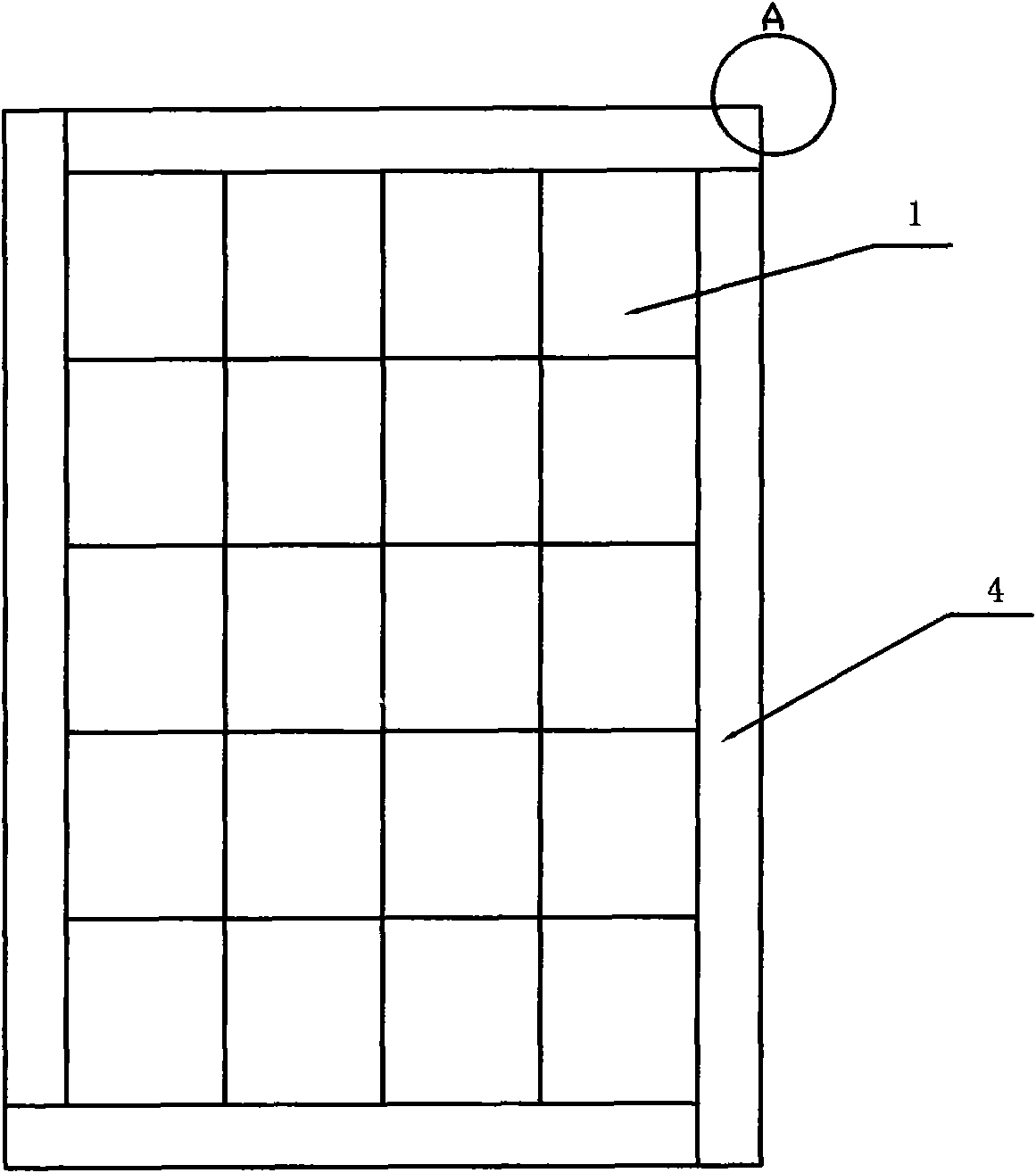
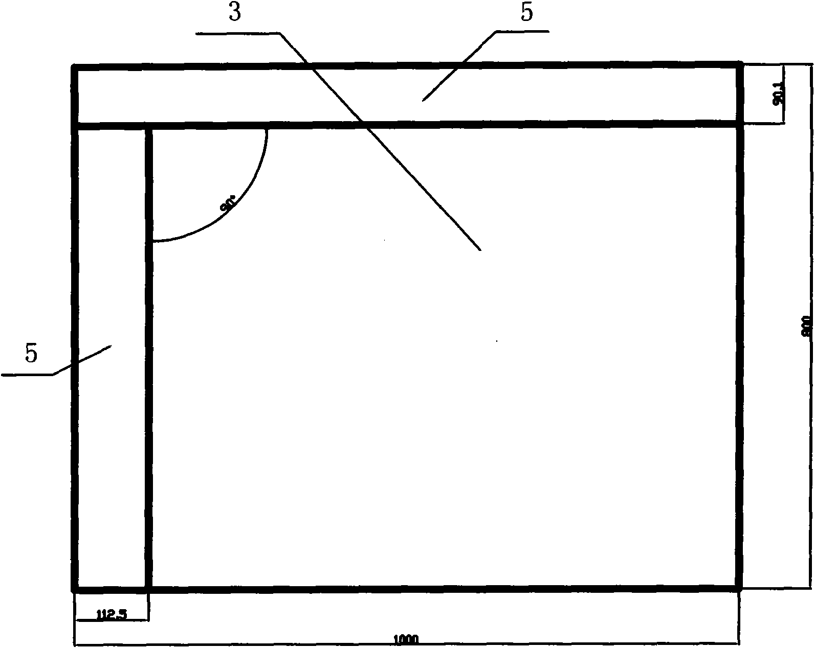
[0030] Task requirements: It is required that the effective molding area of the spliced holographic master is 775X619.8mm, the size of the unit holographic pattern (that is, the small cigarette case) is 155X103.3mm, a total of 30 unit holographic patterns, forming a 5X6 unit holographic pattern The size of the matrix and the holographic master after adding the frame is 1000X800mm. The purpose of the frame (nickel plate with trim) is to meet the requirements of the subsequent process, such as the requirements of electroforming or molding.
[0031] The manufacturing method is:
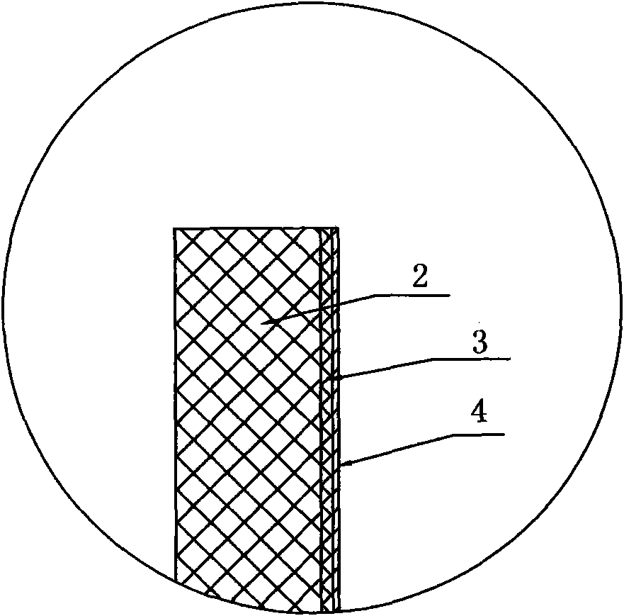
[0032] 1. Copy 30 pieces of holographic patterns (that is, unit holographic patterns) of small cigarette packs by electroforming, that is, copy 30 nickel plates with holographic patterns of small cigarette packs. The thickness of the nickel plates can be selected to be about 55 microns, but each ...
PUM
 Abstract
Description
Claims
Application Information