Electronic packaging method and device

An electronic and packaging technology, applied in circuits, electrical components, transportation and packaging, etc., can solve problems such as insurmountable substrate warpage and transmission problems in the size of the working area, limiting production capacity, etc.

Inactive Publication Date: 2010-01-13
POWERTECH TECHNOLOGY
View PDF0 Cites 0 Cited by
  • Summary
  • Abstract
  • Description
  • Claims
  • Application Information

AI Technical Summary

Problems solved by technology

However, packaging manufacturers use strip-shaped substrates to transfer to each process equipment for the packaging process in order to accommodate the specifications of

Method used


Image

  • Electronic packaging method and device
  • Electronic packaging method and device

Examples


Embodiment Construction

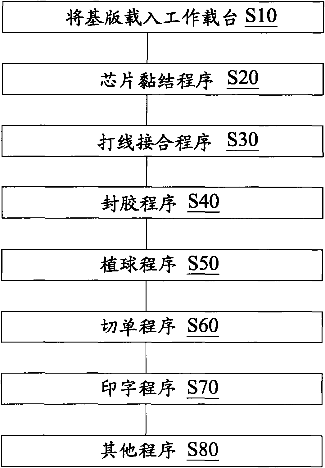
[0010] figure 1 Shown is a schematic flowchart of an electronic assembly method according to an embodiment of the present invention. In this embodiment, firstly, a substrate is loaded on the work platform ( S10 ). Wherein, the substrate can be a full version substrate (panel substrate). Next, a die attach procedure (die attach) is performed to fix a plurality of chips on the substrate (S20). Wherein, the die bonding process is to move a die bonding device, such as a glue dispensing device, a chip grabbing device, etc., to the work platform for operation. Afterwards, a wire bonding process (wire bond) is performed to electrically connect the chip to the substrate by using a plurality of wires ( S30 ). Wherein, the wire bonding procedure is to move a wire bonding device to the work platform for operation.

[0011] Next, a molding process (mold) is performed to cover the chip and the leads ( S40 ). Among them, the sealing procedure is to move the sealing device to the workin...


PUM


Abstract

The invention discloses an electronic packaging method and an electronic packaging device. The method carries out each packaging program by loading a work loading platform to a whole substrate. A plurality of packaging devices are hung near the work loading platform and are moved to an operation position by a mechanical arm. Therefore, problems of warping and transferring of the substrate can be effectively solved. The electronic packaging method and the electronic packaging device can use the whole substrate to carry out the packaging operation and can simultaneously carry out the same or different packaging programs in different areas of the whole substrate so as to effectively increase the yield and reduce the cost.

Description

technical field [0001] The invention relates to an electronic assembly method and its equipment, in particular to an electronic assembly method and its equipment that can use a full board. Background technique [0002] Generally speaking, substrate manufacturers use full panel substrates to manufacture packaging substrates, and before shipment, the full panel substrates are cut into strip type substrates and sent to packaging manufacturers for subsequent packaging operations. However, packaging manufacturers transfer strip substrates to various process equipment for packaging process in order to accommodate the specifications of the original process equipment, so they cannot overcome the size of the working area, substrate warpage and transmission problems, and thus limit the production capacity. Contents of the invention [0003] In order to solve the above problems, one of the objects of the present invention is to provide an electronic packaging method and its equipment...

Claims


Application Information

Patent Timeline
IPC IPC(8): H01L21/00H01L21/50H01L21/677
Inventor 方立志
Owner POWERTECH TECHNOLOGY
Why Eureka
Try Eureka