Non-volatile memory cell and manufacturing method thereof

A non-volatile storage and manufacturing method technology, which is applied in semiconductor/solid-state device manufacturing, electrical components, transistors, etc., can solve the problems of silicon nitride residue, affecting the electrical and stability of components, etc., and improve the gate oxide layer The effect of thinner areas

Active Publication Date: 2010-02-17
NAN YA TECH
View PDF0 Cites 7 Cited by
  • Summary
  • Abstract
  • Description
  • Claims
  • Application Information

AI Technical Summary

Problems solved by technology

However, in the manufacturing method of the vertical dual-bit NAND memory cell of the above-mentioned known technology, in the step of dry etching the ONO dielectric layer 16, silicon nitride residues are likely to be generated at the corners of the side walls, and the manufactured memory cells will have a gate oxide layer. 13 Problems caused by thinner areas, thus affecting the electrical and stability of components

Method used


Image

  • Non-volatile memory cell and manufacturing method thereof
  • Non-volatile memory cell and manufacturing method thereof
  • Non-volatile memory cell and manufacturing method thereof

Examples


Embodiment Construction

[0023] Use the following Figure 2(A) to Figure 2(M) Embodiments of the manufacturing method of the non-volatile memory cell of the present invention will be described.

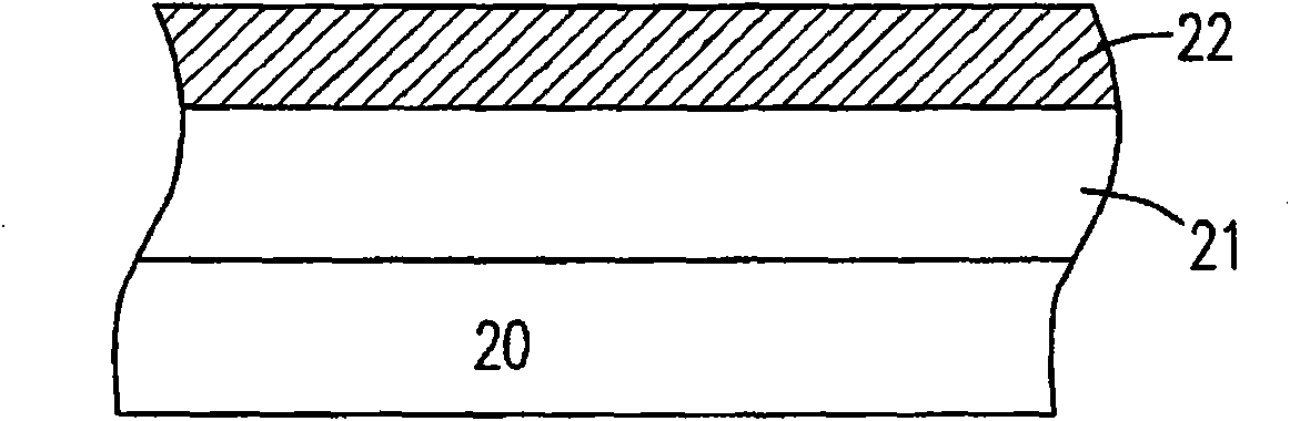
[0024] 2(A), a semiconductor substrate 20 is provided, the semiconductor substrate 20 is, for example, a silicon substrate, a conductive layer 21 is formed on the semiconductor substrate 20, and a spacer layer 22 is formed on the conductive layer 21 , wherein the spacer layer 22 may be composed of silicon nitride.

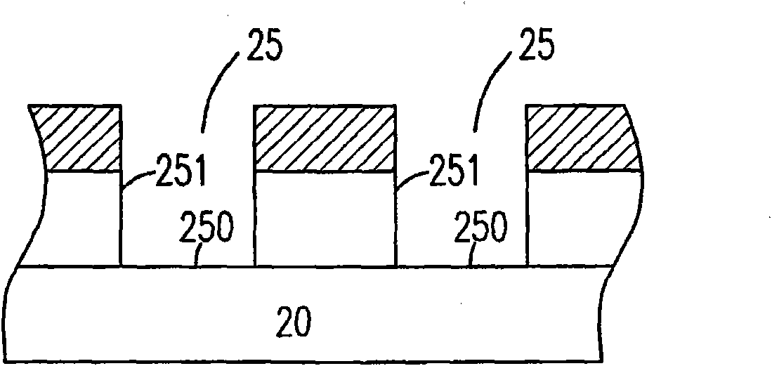
[0025] Next, referring to FIG. 2(B), a portion of the spacer layer 22 and the conductive layer 21 are etched to the top of the semiconductor substrate 20 to form at least one trench 25. As shown in the figure, each trench 25 includes the bottom of the trench 250 and sidewalls 251 of the trench.

[0026] 2(C), a first oxide layer 23 is formed on the bottom 250 of the trench 25. In this embodiment, an oxide layer is deposited by chemical vapor deposition (CVD) method, and then removed by etching. ...


PUM


Abstract

The invention provides a non-volatile memory cell and a manufacturing method thereof. The method comprises the following steps: providing a semiconductor substrate which is provided with a conductivelayer and a spacer layer in order; defining at least one trench between the spacer layer and the conductive layer; forming a first oxidization layer at the bottom of the trench; forming a dielectric layer on the side wall of the trench, above the first oxidization layer and above the spacer layer; forming a first polysilicon layer in the trench; and removing the dielectric layer above the spacer layer to form the basic structure of the non-volatile memory cell of the invention.

Description

technical field [0001] The present invention relates to a non-volatile memory cell and a manufacturing method thereof, in particular to a vertical dual-bit NAND memory cell and a manufacturing method thereof. Background technique [0002] Flash memory (Flash) is the mainstream of non-volatile memory, mainly divided into NOR Flash and NAND Flash, among which NAND Flash is especially suitable for a large amount of data storage due to its high density and high writing speed. With the rise of portable multimedia storage devices, the market demand for NAND Flash has greatly increased. Therefore, the industry is constantly researching and improving process technology to reduce the size of components and improve product reliability. [0003] The traditional memory structure is to form flat memory cells on a silicon substrate, and the copy process must be repeated according to the number of layers designed. Therefore, it is difficult to reduce the cost due to the increase in the num...

Claims


Application Information

Patent Timeline
Patent Type & Authority Applications(China)
IPC IPC(8): H01L21/28H01L21/336H01L21/8247H01L29/423H01L29/788H01L27/115
Inventor 黄信斌萧清南黄仲麟
Owner NAN YA TECH
Why Eureka
Try Eureka