

Semiconductor storage device
A storage device and semiconductor technology, applied in the direction of information storage, static memory, digital memory information, etc., can solve the problems of increased reading speed degradation, etc., and achieve the reduction of bit line load capacitance, large capacity, and large area reduction effect Effect
- Summary
- Abstract
- Description
- Claims
- Application Information
AI Technical Summary
Problems solved by technology
Method used
Image

Examples
Embodiment approach 1
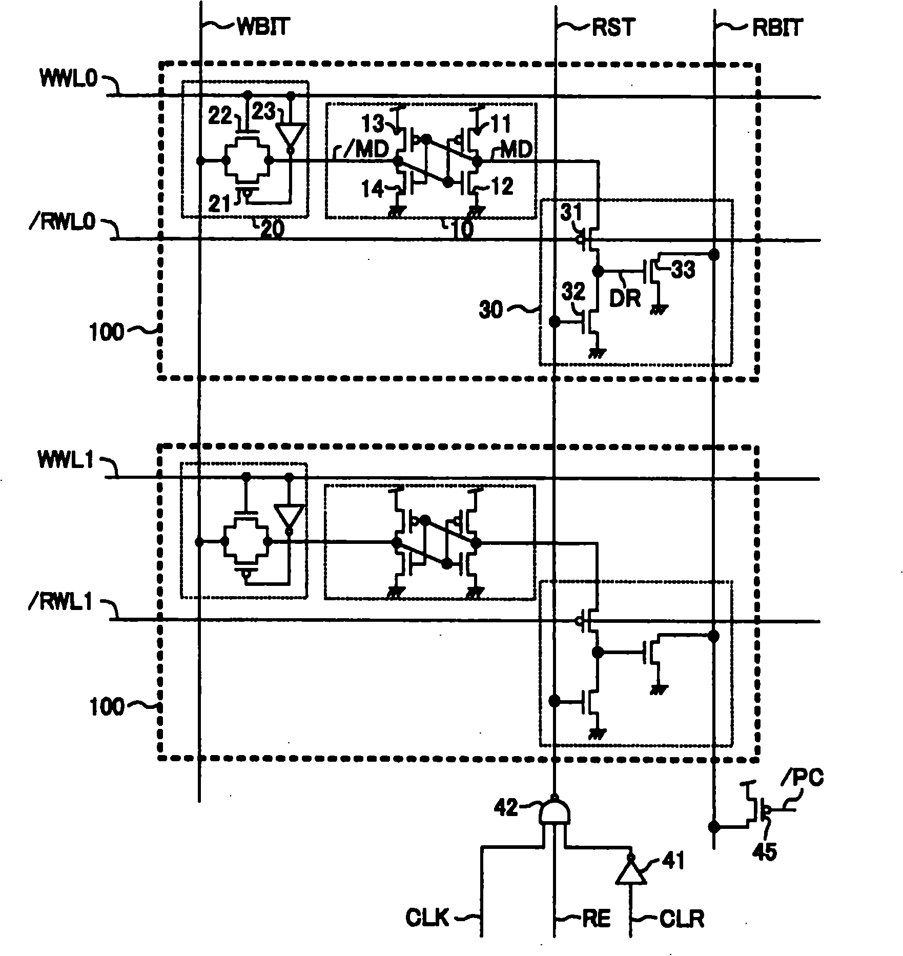
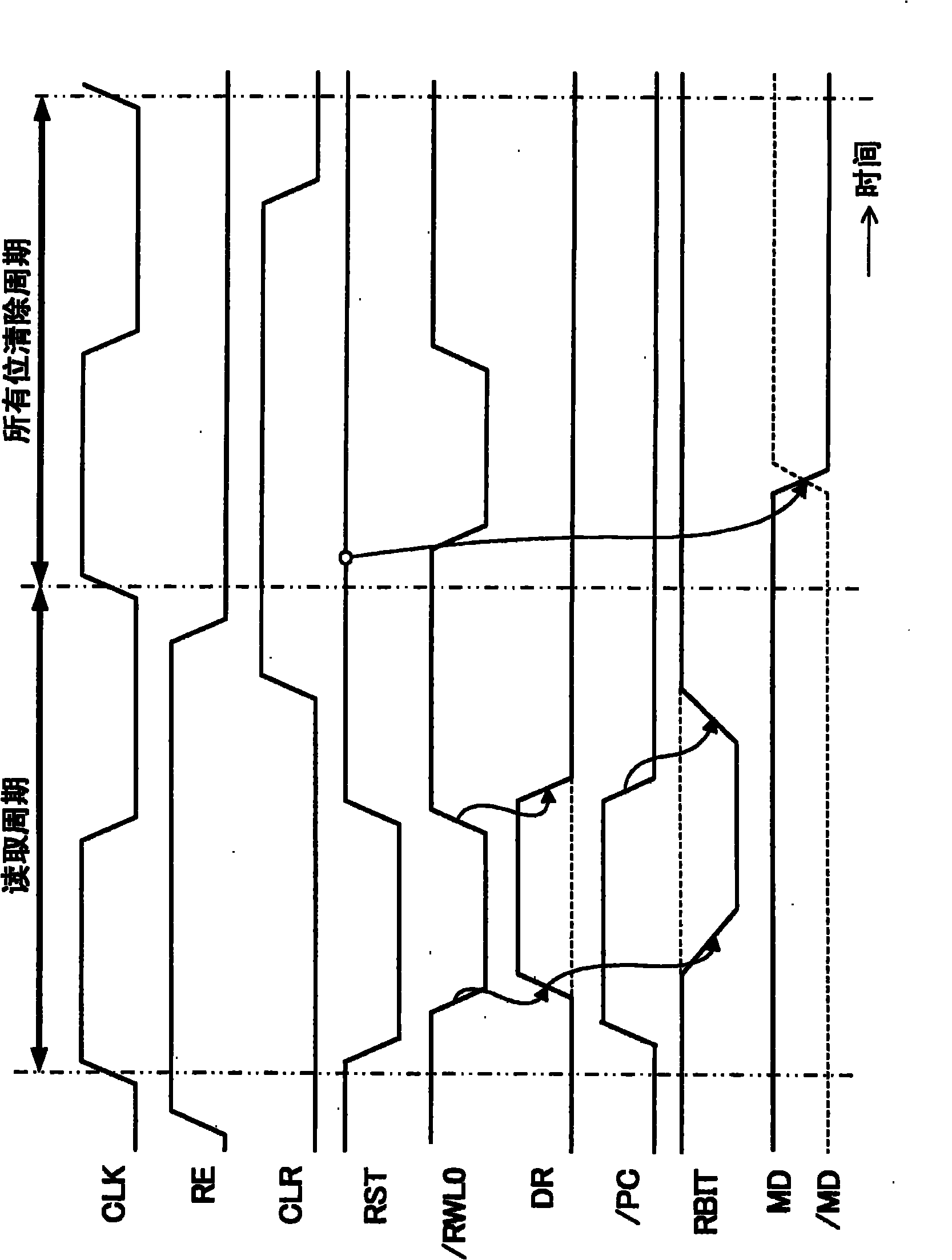
[0029] figure 1 It is a circuit diagram of the semiconductor memory device according to Embodiment 1 of the present invention. figure 1 The semiconductor memory device includes a plurality of memory cells 100 that share a write bit line WBIT and a read bit line RBIT. Each memory cell 100 includes a memory circuit 10 that stores data, a write circuit 20 that writes data into the memory circuit 10 , and a read circuit 30 that reads data from the memory circuit 10 .
[0030] The memory circuit 10 has a PMOS transistor 11 and an NMOS transistor 12 constituting a first inverter, and a PMOS transistor 13 and an NMOS transistor 14 constituting a second inverter. The output node of the first inverter is connected to the input of the second inverter as the data holding node MD on the TRUE side, and the output node of the second inverter is connected to the input of the first inverter as the data holding node / MD on the BAR side .
[0031] The write circuit 20 has a PMOS transistor 2...
Embodiment approach 2
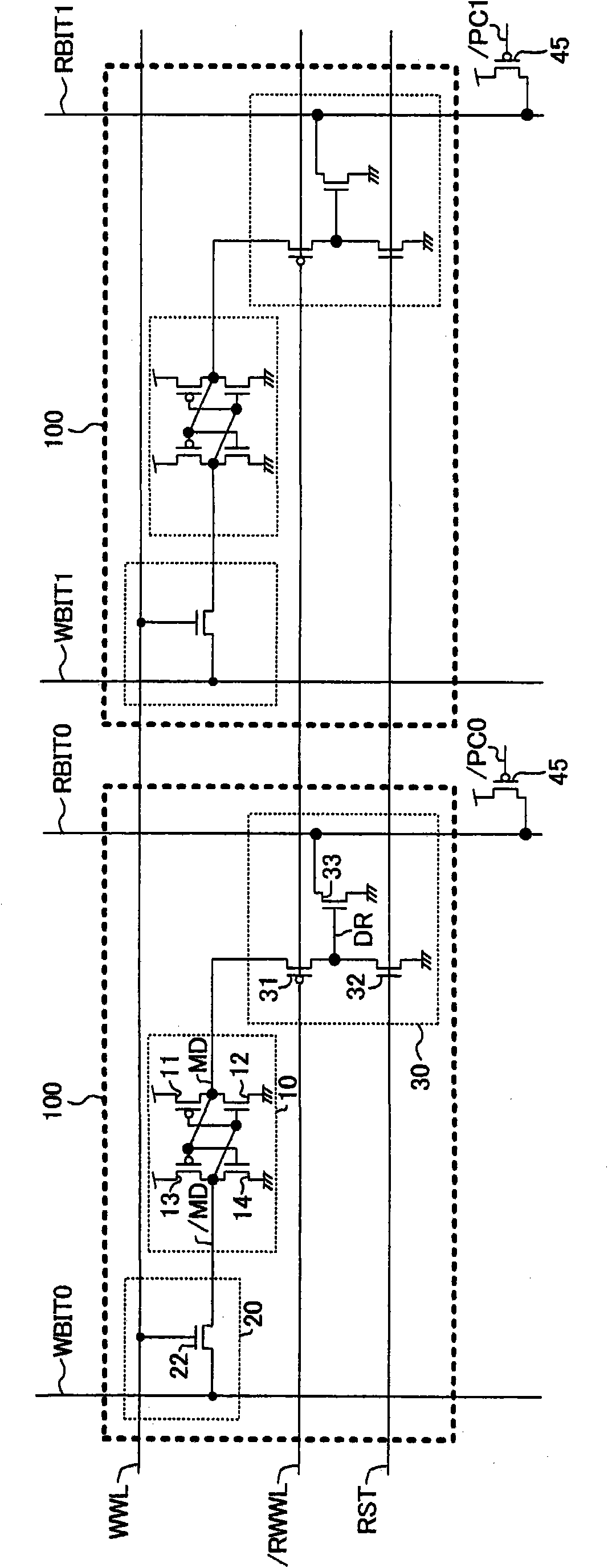
[0044] image 3 It is a circuit diagram of a semiconductor memory device according to Embodiment 2 of the present invention. image 3 The structural feature of the above is that the reset control signal RST is shared among multiple memory cells 100 connected to the same write word line WWL and the same read / write word line / RWWL. image 3 WBIT0 and RBIT0 in are the write bit line and read bit line for bit 0, respectively, and WBIT1 and RBIT1 are the write bit line and read bit line for bit 1, respectively. / PC0 and / PC1 are precharge control signals.
[0045] exist image 3 In the configuration described above, after the memory circuit 10 is initialized using the reset transistor 32 , writing of desired data is performed using the write circuit 20 . The advantage of this structure is that since the memory circuit 10 on the read / write word line / RWWL to be written is initialized by using the reset transistor 32 before writing, the write circuit 20 only needs to have the data ...
Embodiment approach 3
[0052] Figure 5 It is a circuit diagram of a semiconductor memory device according to Embodiment 3 of the present invention. exist Figure 5 Among them, 50 is a read and write circuit. The read / write circuit 50 not only has a switching transistor 31 connected to the TRUE side data holding node MD of the storage circuit 10 and the transistor control line DR for output wiring driving during reading and writing, but also includes a transistor control line DR for output wiring driving. The reset function also includes a reset transistor 32 for initializing the storage circuit 10, an output wiring driving transistor 33 connected to the read bit line RBIT, and a reset function for writing and initializing the storage circuit 10. The opposite data writing transistor 51 . / RWWL0 and / RWWL1 are the read and write word lines. In addition, DI is an input data signal, WE is a write enable signal, PLS is a pulse signal, 61 and 63 are AND gate circuits, and 62 is a NAND gate circuit. ...
PUM
 Abstract
Description
Claims
Application Information