Induction structure and touch display panel

A touch display panel and main sensing technology, applied in the field of touch display panel and resistive sensing structure, can solve problems such as the deterioration of the sensing capability of the touch panel, achieve good sensing capability and improve the sensing capability. Effect

Inactive Publication Date: 2010-07-28
AU OPTRONICS CORP
View PDF3 Cites 3 Cited by
  • Summary
  • Abstract
  • Description
  • Claims
  • Application Information

AI Technical Summary

Problems solved by technology

For example, the greater the thickness of the alignment material layer remaining on the touch conductor and the touch pad, the greater the minimum external force (active force) that can sense touch, that is, the greater the sensing capability of the touch panel. Difference

Method used


Image

  • Induction structure and touch display panel
  • Induction structure and touch display panel
  • Induction structure and touch display panel

Examples


Embodiment Construction

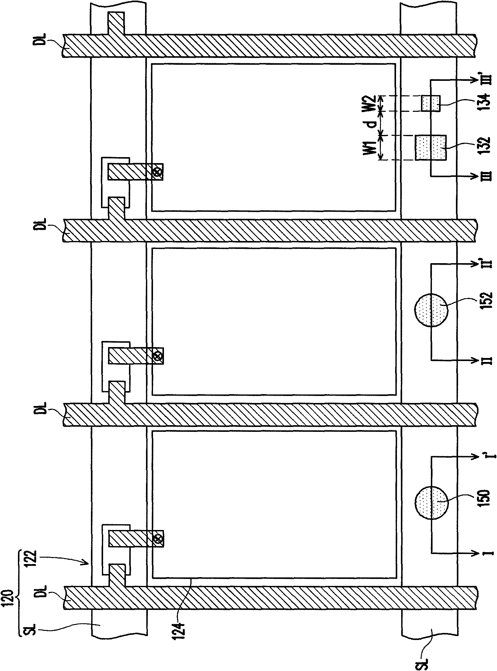
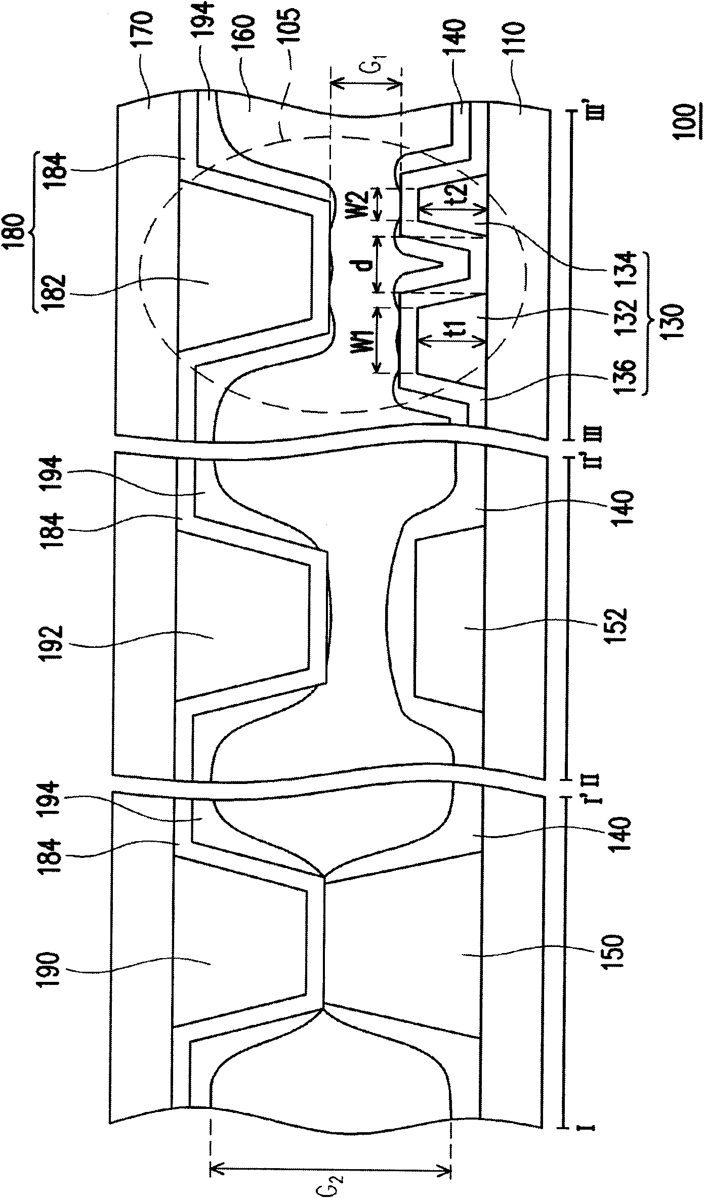
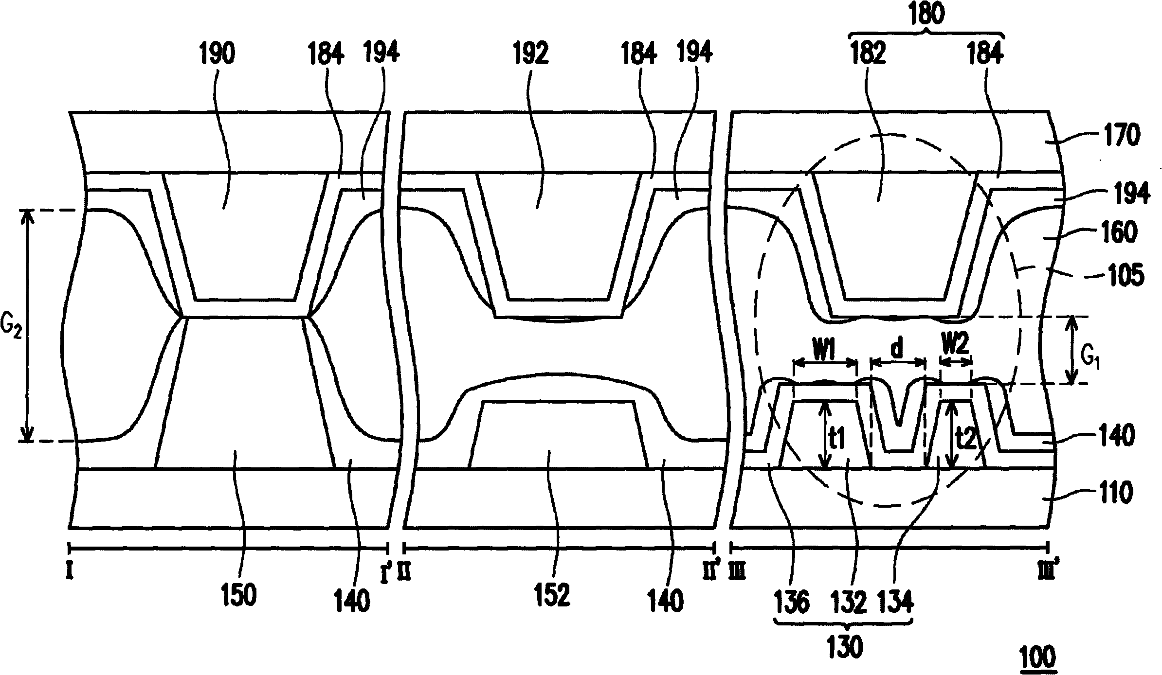
[0024] figure 1 is a schematic top view of a touch display panel according to an embodiment of the present invention. figure 2 is corresponding to figure 1 Schematic cross-sectional views of I-I', II-II' and III-III'. Among them, for the sake of illustration clarity, figure 1 Only a schematic top view of the first substrate of the touch display panel of this embodiment is shown, and no figure 2 in the second substrate. Please refer to figure 1 as well as figure 2 The touch display panel 100 of this embodiment is, for example, a built-in touch display panel, which includes a first substrate 110 , a second substrate 170 and a display medium 160 between the two substrates 110 , 170 . Wherein, the display medium 160 includes liquid crystal molecules or other display mediums.

[0025] In this embodiment, the first substrate 110 is, for example, an active device array substrate, on which the active device array layer 120 and multiple sets of sensing units 130 are disposed....


PUM


Abstract

The invention discloses a touch display panel which comprises first substrate and a second substrate. The first substrate comprises a plurality of induction units, each induction unit is provided with a main induction pattern and at least one primary induction pattern, wherein the at least one primary induction pattern is electrically connected with the main induction pattern, and the size of the at least one primary induction pattern is smaller than that of the main induction patter. The second substrate comprises a plurality of induction electrodes, and each induction electrode is arranged corresponding to one induction unit on the first substrate.

Description

technical field [0001] The present invention relates to a sensing structure, and in particular to a resistive sensing structure and a touch display panel with the resistive sensing structure. Background technique [0002] In general touch display panel design, it can be roughly classified into capacitive, resistive, photosensitive, etc. based on the design principle of the touch sensing mode; ) and built-in (integrated type) two. Among them, the built-in resistive touch panel forms a plurality of touch conductors on the opposite substrate and a photo spacer, and forms a plurality of touch pads on the active device array substrate. When the user presses the opposite When connecting the substrate, the touch conductor on the spacer can be connected to the touch pad on the active device array substrate, so as to locate the position pressed by the user. Therefore, the gap between the touch conductor and the touch pad will affect the sensing capability of the touch panel. [00...

Claims


Application Information

Patent Timeline
Patent Type & Authority Applications(China)
IPC IPC(8): G06F3/041
Inventor 程琮钦吴岳鸿陈政德李锡烈
Owner AU OPTRONICS CORP
Why Eureka
Try Eureka