Organic light emitting diode display
A light-emitting diode and display technology, which is applied to static indicators, instruments, identification devices, etc., can solve problems such as uneven brightness of pixels
- Summary
- Abstract
- Description
- Claims
- Application Information
AI Technical Summary
Problems solved by technology
Method used
Image
Examples
no. 1 example
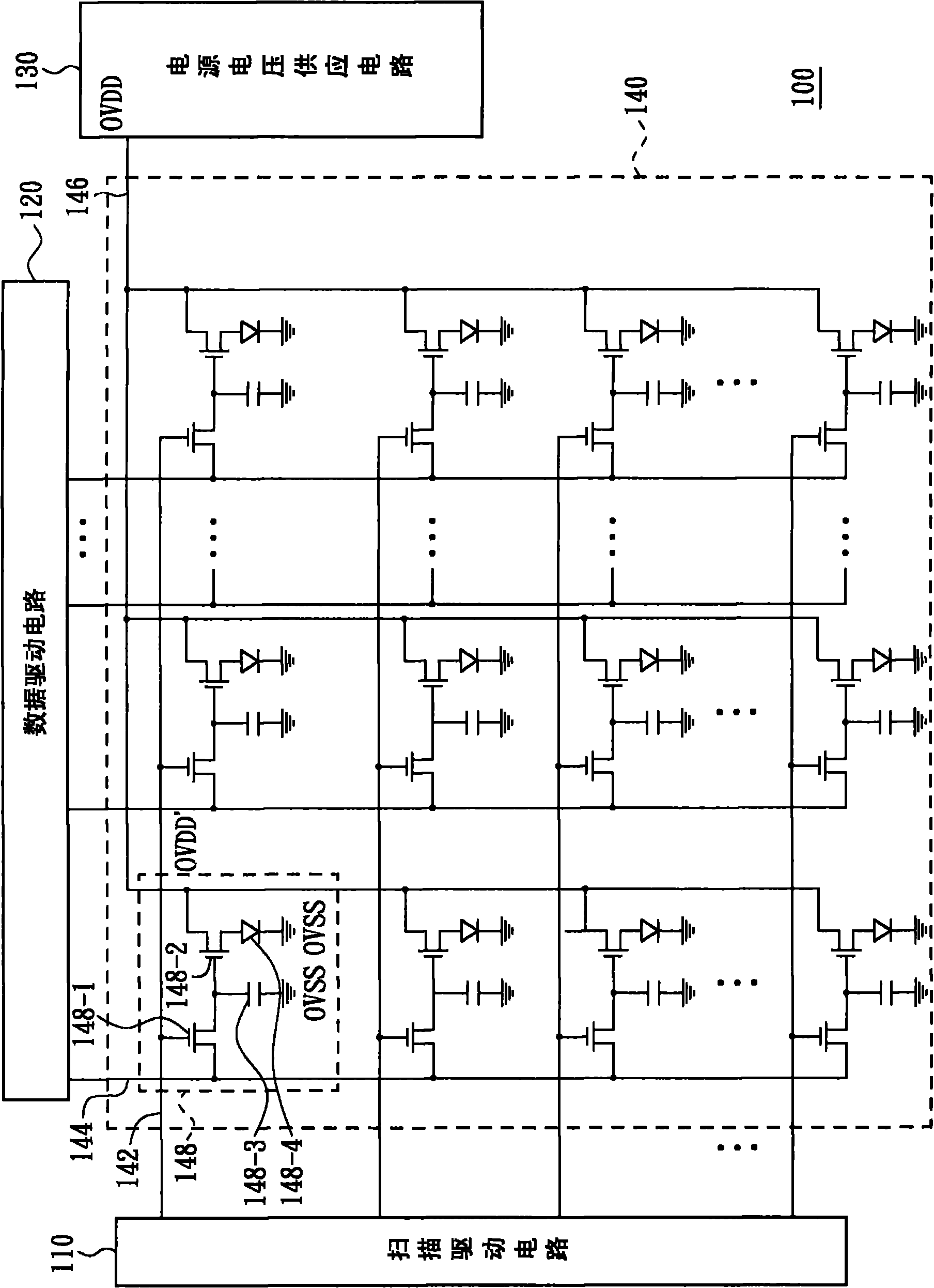
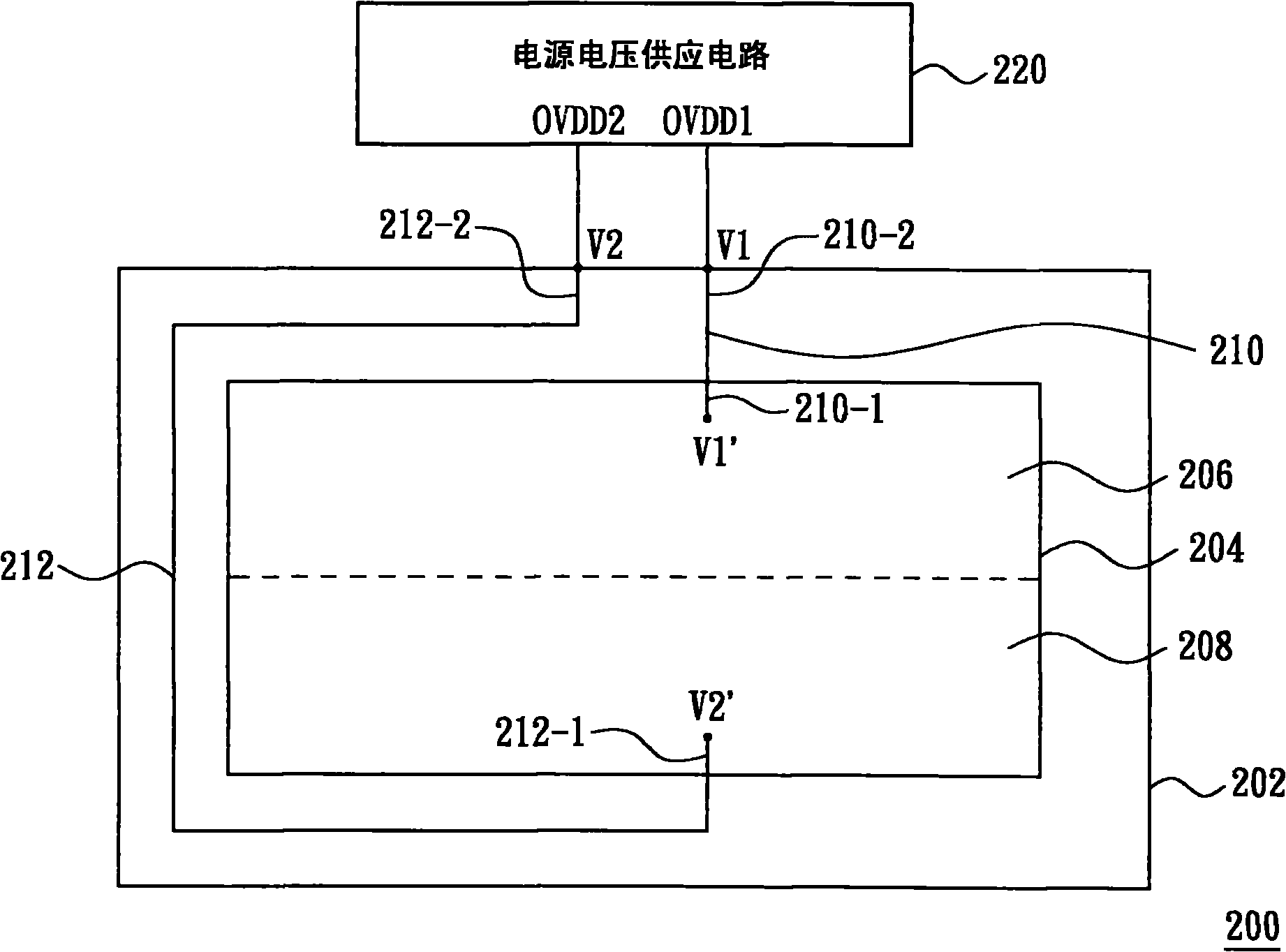
[0039] figure 2 It is a schematic diagram of an organic light emitting diode display according to an embodiment of the invention. this figure 2 The organic light emitting diode display 200 shown only shows figure 1 The different parts of the organic light emitting diode display 100 shown are omitted, and other similar parts are omitted to avoid redundant description and confusion of the key points of the present invention.
[0040] Such as figure 2 As shown, the organic light emitting diode display 200 mainly includes an organic light emitting diode display panel 202, wires 210, wires 212, and a power supply voltage supply circuit 220. The organic light emitting diode display panel 202 has a display area 204 formed by a plurality of pixels (not shown), and the display area 204 is divided into a sub-display area 206 and a sub-display area 208. In this example, the area size of the sub-display area 206 and the area size of the sub-display area 208 are the same. However, the are...
no. 2 example
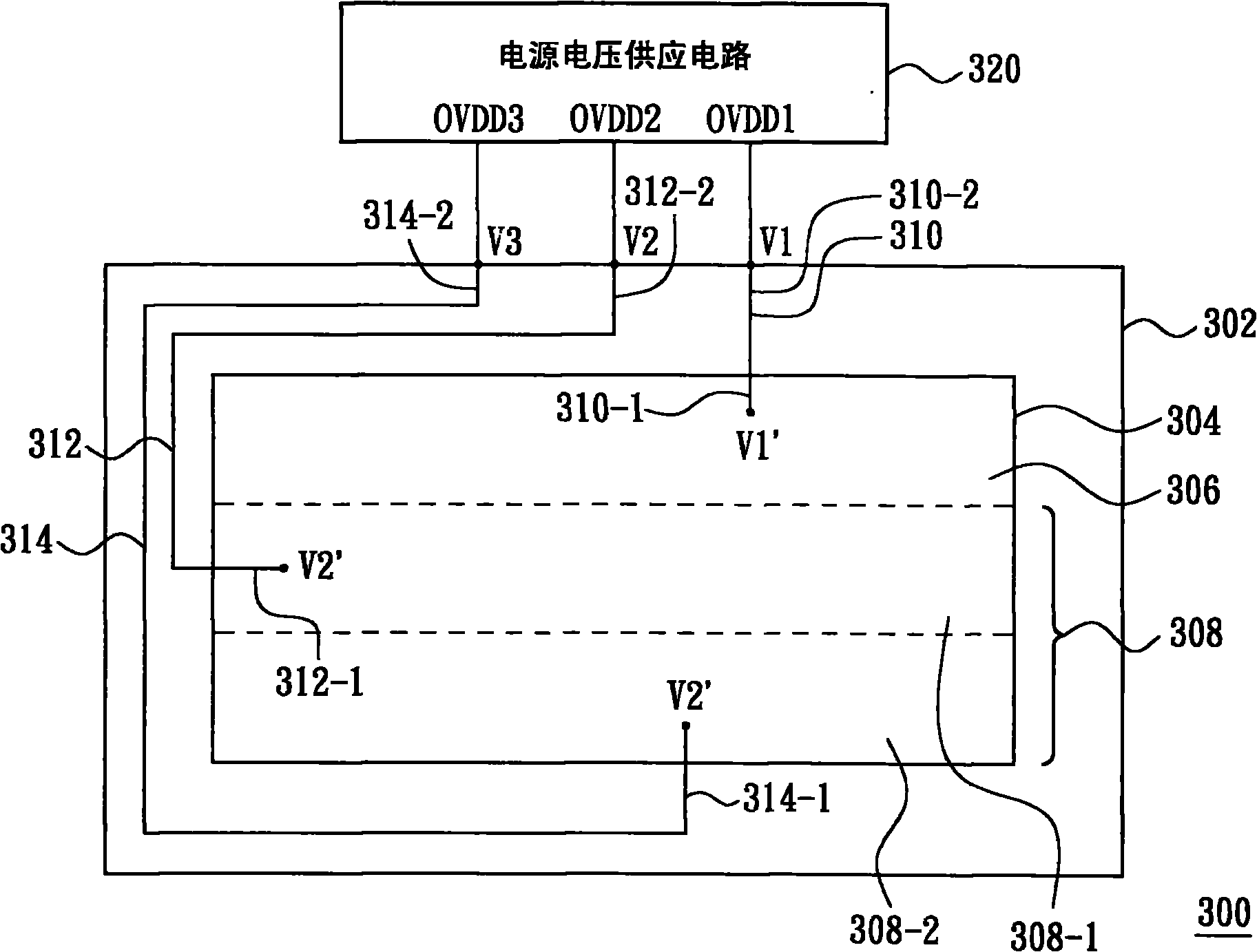
[0049] image 3 It is a schematic diagram of an organic light emitting diode display according to another embodiment of the invention. Please refer to image 3 The organic light emitting diode display 300 mainly includes an organic light emitting diode display panel 302, wires 310, wires 312, wires 314, and a power supply voltage supply circuit 320. The display area 304 of the organic light emitting diode display panel 302 is divided into sub-display areas 306 and 308, and the sub-display area 308 is divided into sub-display areas 308-1 and 308-2. In this example, the area size of the sub display area 306, the area size of the second sub display area 308-1, and the area size of the second sub display area 308-2 are the same. However, the size of the three areas can also be different.
[0050] The above three wires are all disposed on the organic light emitting diode display panel 302 and located outside the display area 304, and the first end 310-1 of the wire 310 is electricall...
no. 3 example
[0055] Figure 4 It is a schematic diagram of an organic light emitting diode display according to another embodiment of the present invention. Please refer to Figure 4 The organic light emitting diode display 400 mainly includes an organic light emitting diode display panel 402, wires 410, wires 412, wires 414, wires 416, and a power supply voltage supply circuit 420. The display area 404 of the organic light emitting diode display panel 402 is divided into sub-display areas 406 and 408. The sub-display area 406 is divided into sub-display areas 406-1 and 406-2, and the sub-display area 408 is divided into sub-display areas 406-1 and 406-2. Display areas 408-1 and 408-2. In this example, the areas of the four sub-display areas are the same. However, in practical applications, the area sizes of the four sub-display areas can also be different.
[0056] The above four wires are all disposed on the organic light emitting diode display panel 402 and located outside the display ...
PUM
 Abstract
Description
Claims
Application Information


