Group III nitride semiconductor light-emitting device, method for manufacturing the same, and lamp
A technology of nitride semiconductors and light-emitting elements, which is applied in the direction of semiconductor devices, electrical components, and electric solid-state devices. It can solve the problems of stacked crystals and instability, and achieve the effects of improved crystallinity and excellent luminous characteristics.
- Summary
- Abstract
- Description
- Claims
- Application Information
AI Technical Summary
Problems solved by technology
Method used
Image

Examples
Embodiment 1
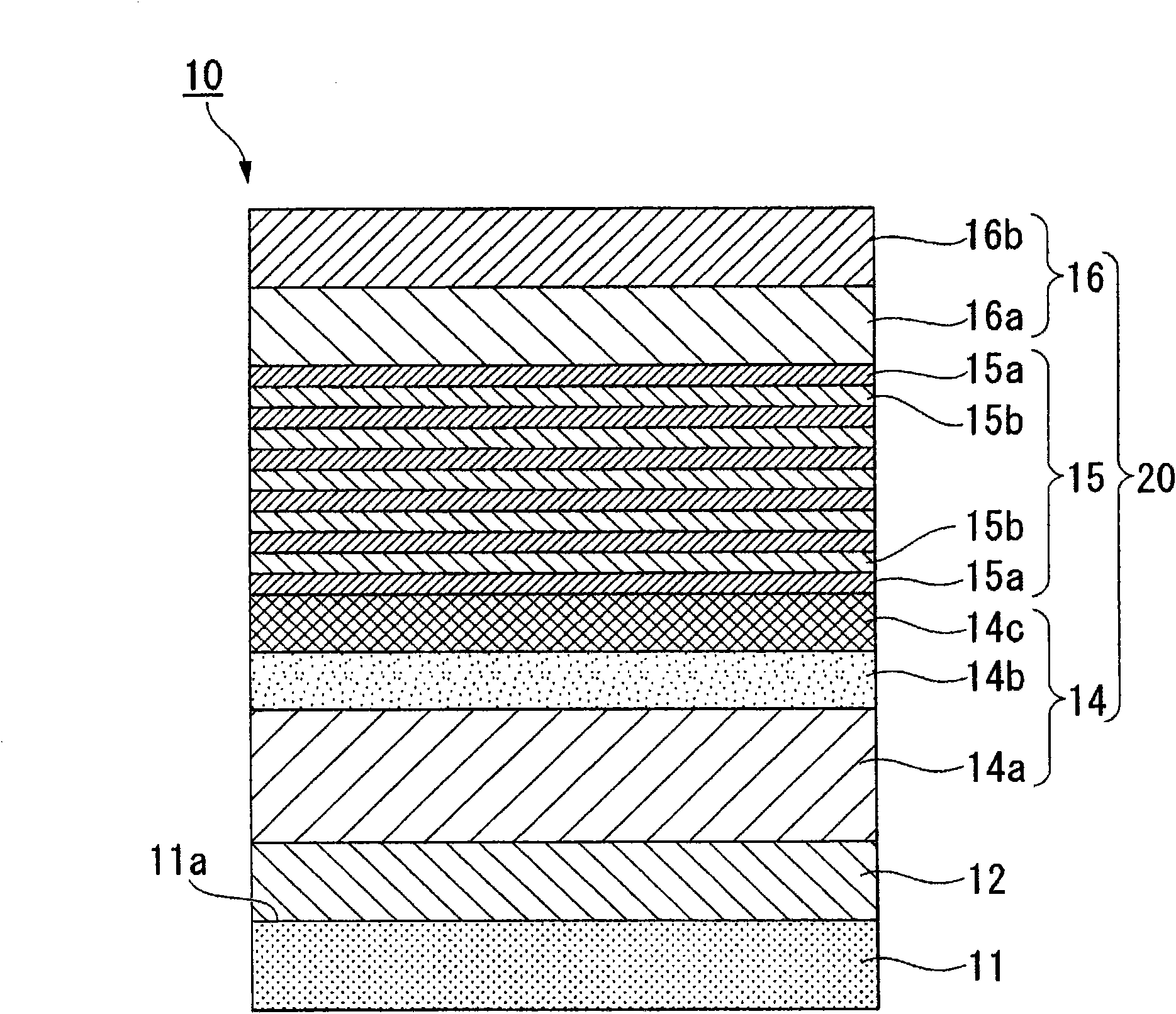
[0222] figure 1 A schematic cross-sectional view showing a stacked semiconductor of a group III nitride compound semiconductor light-emitting device produced in this experimental example.
[0223] In this example, on the c-plane of the substrate 11 made of sapphire, a single crystal layer made of AlN was formed as the buffer layer 12 by RF sputtering method, and GaN made of GaN was formed on the buffer layer by reactive sputtering method. A layer made of (III nitride semiconductor) serves as the base layer 14a.
[0224] "Formation of the buffer layer"
[0225] First, a substrate made of (0001) c-plane sapphire with a mirror-polished surface of 2 inches in diameter was washed with hydrofluoric acid and an organic solvent, and introduced into a chamber. At this time, as a sputtering device, such as Figure 5 The illustrated sputtering apparatus 40 has a high-frequency power supply and a mechanism capable of moving the position of the magnet within the target. In addition, as t...
Embodiment 2
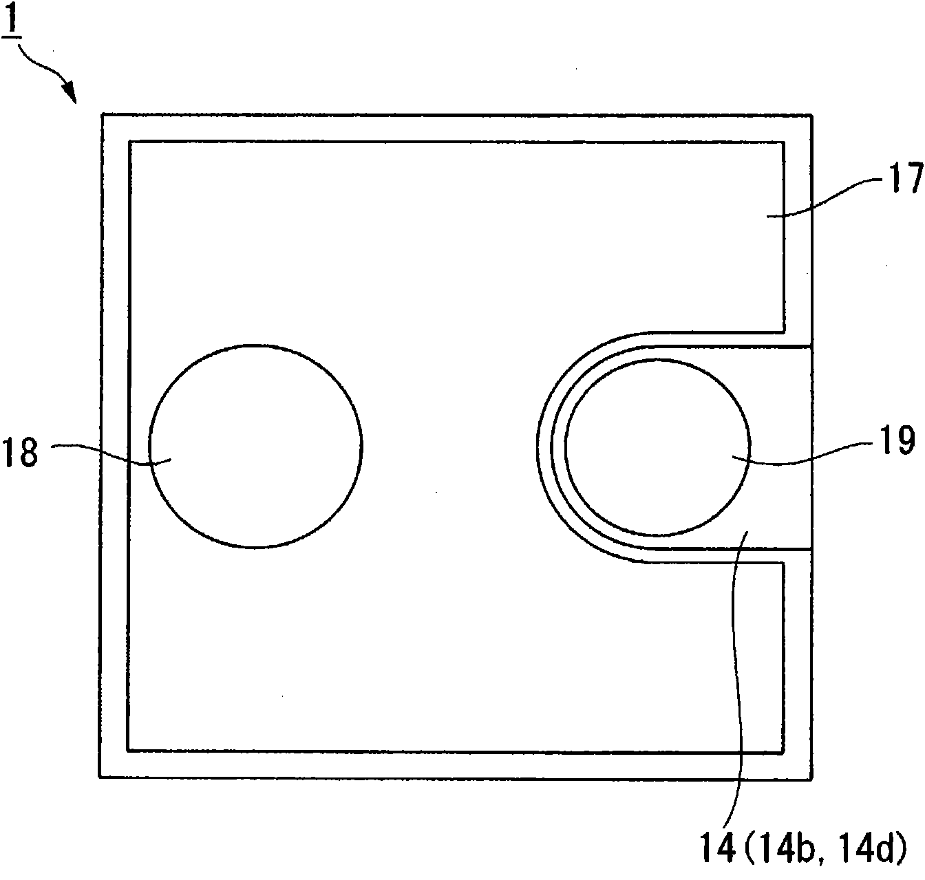
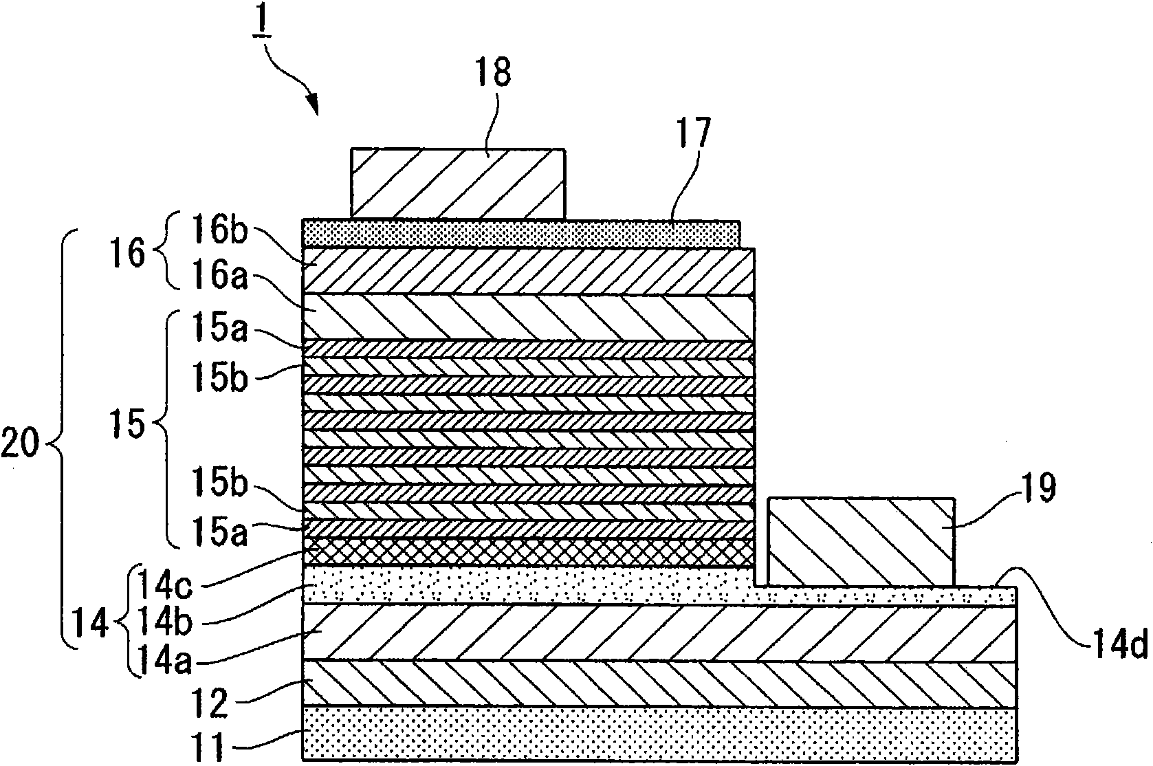
[0262] The buffer layer deposited on the substrate was laminated on the substrate in the same manner as in Example 1 except that the crystal structure of the buffer layer formed on the substrate was polycrystalline with a columnar crystal texture. layer, on which an undoped GaN layer (base layer) is laminated, and further, each layer including a group III nitride semiconductor is formed, thereby making such a figure 2 and image 3 The light emitting element shown.
[0263] The X-ray rocking curve (XRC) of the buffer layer formed on the substrate was measured by the same method as in Example 1, and the XRC half value width was 12 arcsec. In addition, the composition of the buffer layer was measured using an X-ray photoelectron spectroscopy (XPS), and similar to Example 1, it was confirmed that the oxygen concentration was 1% or less in atomic %.
[0264] Next, by the same method as in Example 1, a GaN layer was formed on the buffer layer formed on the substrate by the reacti...
experiment example
[0276] Hereinafter, regarding experimental examples for demonstrating the present invention, use Figure 7A , 7B Each figure will be described. Figure 7A is a graph showing the relationship between the number of dummy discharges and the oxygen concentration in the buffer layer, Figure 7B It is a graph showing the relationship between the degree of vacuum attained in the chamber and the oxygen concentration in the buffer layer.
[0277] In this experimental example, after the pretreatment of the substrate, the Figure 7A The number of times shown is to use the vacuum pump to remove the dummy discharge when the chamber is pumped to remove impurities, and the attained vacuum degree in the chamber is set as Figure 7B The conditions shown (No.1=2.0×10 -5 Pa, No.2=3.1×10 -5 Pa, No.3=5.1×10 -5 Pa, No.4=1.5×10 -4 Pa), each sample of No. 1-4 which formed the buffer layer on the board|substrate by the method similar to Example 1 about the point other than this was produced.
...
PUM
 Abstract
Description
Claims
Application Information
 - R&D Engineer
- R&D Manager
- IP Professional
- Industry Leading Data Capabilities
- Powerful AI technology
- Patent DNA Extraction
Browse by: Latest US Patents, China's latest patents, Technical Efficacy Thesaurus, Application Domain, Technology Topic.
© 2024 PatSnap. All rights reserved.Legal|Privacy policy|Modern Slavery Act Transparency Statement|Sitemap