Frequency jitter circuit and frequency jitter generating method

A technology of frequency jitter and circuit, applied in the direction of electric pulse generator circuit, differential amplifier to generate pulse, electrical components, etc., can solve the problems of external chip, increase of PCB board volume and cost, etc., and achieve the effect of simple circuit and easy realization

Active Publication Date: 2012-05-23
HANGZHOU SILAN MICROELECTRONICS
View PDF0 Cites 0 Cited by
  • Summary
  • Abstract
  • Description
  • Claims
  • Application Information

AI Technical Summary

Problems solved by technology

In practice, filtering methods are often used to reduce electromagnetic interference, but external capacitors and inductors are required on the chip, which increases the size and cost of the PCB board

Method used


Image

  • Frequency jitter circuit and frequency jitter generating method
  • Frequency jitter circuit and frequency jitter generating method
  • Frequency jitter circuit and frequency jitter generating method

Examples


Embodiment Construction

[0047] The content of the present invention will be further described below in conjunction with the accompanying drawings.

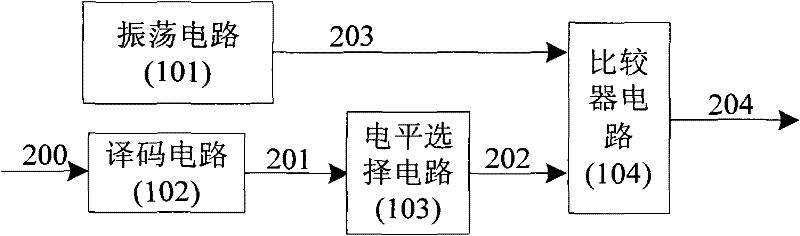
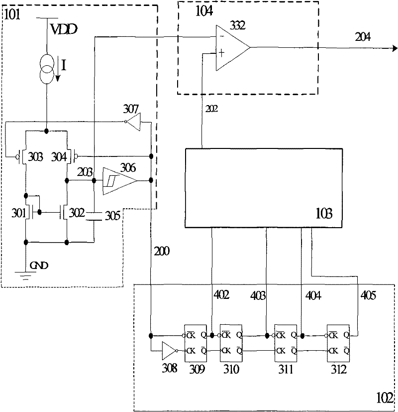
[0048] Such as figure 1 As shown, it is a structural diagram of the frequency dithering circuit 100 of the present invention, including:

[0049] An oscillation circuit 101, the oscillation circuit 101 generates a sawtooth wave signal 203;

[0050] Decoding circuit 102, the oscillating frequency signal 200 is input into the decoding circuit 102, and the decoding circuit 102 is controlled to generate several pulse signals 201;

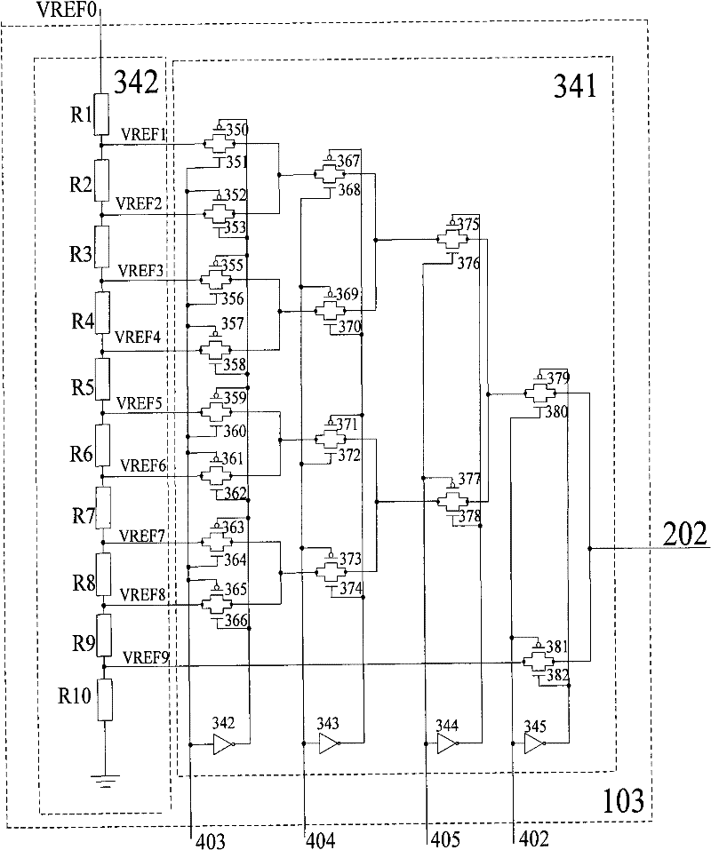
[0051] A level selection circuit 103, the pulse signal 201 controls the level selection circuit 103 to generate an output level signal 202 that varies with the pulse output signal 201;

[0052] The comparator circuit 104 compares the sawtooth wave signal 203 and the output level signal 202 to generate a frequency jitter signal 204. With the change of the output level signal 202, the duty cycle of the frequency jitter signal 204 ...


PUM


Abstract

The invention provides a frequency jitter circuit, comprising an oscillating circuit, a decoding circuit, a level selecting circuit and a comparator circuit, wherein the oscillating circuit is used for generating a sawtooth signal; an oscillation frequency signal is input into the decoding circuit and controls the decoding circuit to generate a plurality of pulse signals; the pulse signals control the level selecting circuit to generate an output level signal which varies along with variation of a pulse output signal; the comparator circuit is used for comparing the sawtooth signal of the oscillation frequency and the output level signal and generating a frequency jitter signal; and the duty ratio of the frequency jitter signal and the edge of turn-on / turn-off vary along with variation ofthe output level signal. The invention also provides a method for generating frequency jitter. The frequency jitter circuit provided by the invention has the advantages of simple lines and easy realization. Meanwhile, frequency jitter ensures the switching frequency to be in a wide frequency range, ensures the EMI energy measured by EMI equipment to be diffused beyond the bandwidth, reduces the average EMI noises and flattens the energy spectrum density of the EMI noises.

Description

technical field [0001] The invention relates to the field of switching power supplies, in particular to a frequency jitter circuit in an integrated circuit and a method for generating frequency jitter. Background technique [0002] Due to the high-frequency switching of the switching power supply voltage regulator circuit, the circuit generates electromagnetic interference (EMI). EMI noise can be transmitted through the input AC power line, and can also be transmitted through radiation, which will affect other electronic instruments, such as communication tools, The normal work of household appliances, automatic control equipment, etc. [0003] In order to control the electromagnetic interference (EMI), the control standard limits the energy requirements of the radiation, so as to ensure that the normal operation of various instruments will not be affected by mutual interference. In practice, filtering methods are often used to reduce electromagnetic interference, but exter...

Claims


Application Information

Patent Timeline
Patent Type & Authority Patents(China)
IPC IPC(8): H02M1/44H03K3/023
Inventor 姚云龙
Owner HANGZHOU SILAN MICROELECTRONICS
Why Eureka
Try Eureka