Embedded substrate provided with side-inclined plane line layer assembly and manufacturing method thereof

A circuit layer, embedded technology, applied in the direction of printed circuit components, electrical connection printed components, printed components electrical connection formation, etc., can solve problems such as inconvenience

Active Publication Date: 2012-07-25
ADVANCED SEMICON ENG INC
View PDF0 Cites 2 Cited by
  • Summary
  • Abstract
  • Description
  • Claims
  • Application Information

AI Technical Summary

Problems solved by technology

However, in order to form the positioning block 18, more considerations must be made when designing the circuit, which causes inconvenience

Method used


Image

  • Embedded substrate provided with side-inclined plane line layer assembly and manufacturing method thereof
  • Embedded substrate provided with side-inclined plane line layer assembly and manufacturing method thereof
  • Embedded substrate provided with side-inclined plane line layer assembly and manufacturing method thereof

Examples


Embodiment Construction

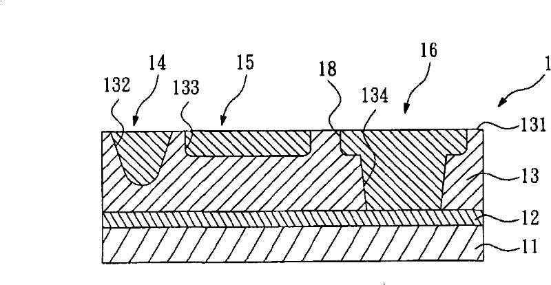
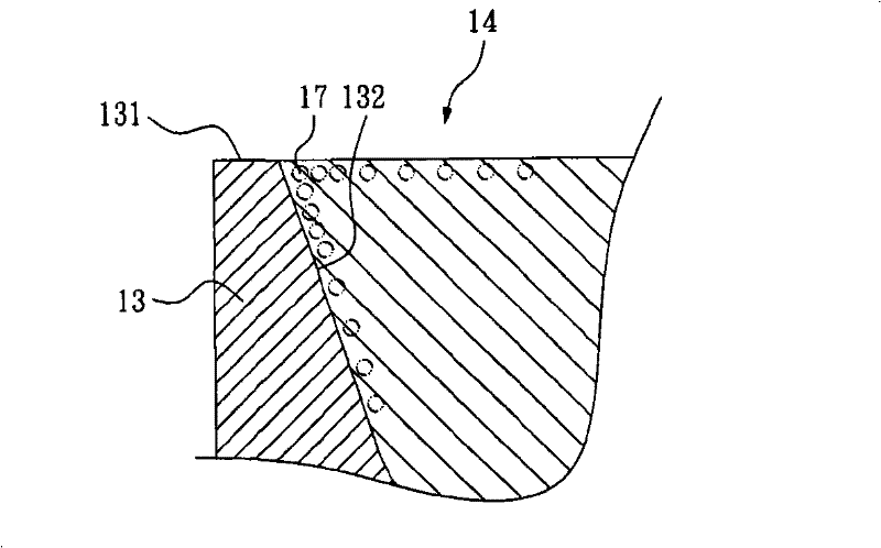
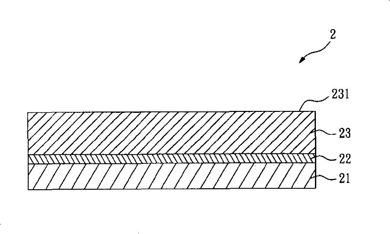
[0049] refer to Figure 3 to Figure 8 , is a schematic diagram showing a method for manufacturing an embedded substrate of a circuit layer assembly with side bevels according to the present invention. refer to image 3 , providing a substrate 2 including a dielectric layer 23 having an upper surface 231 . In this embodiment, the substrate 2 further includes a core layer 21 and a first copper layer 22 , the first copper layer 22 is located on the core layer 21 , and the dielectric layer 23 is located on the first copper layer 22 .

[0050] refer to Figure 4 , removing part of the dielectric layer 23 from the upper surface 231 of the dielectric layer 23 to form at least one accommodating groove 232, 233, 234, and these accommodating grooves 232, 233, 234 are opened on the upper surface 231, And viewed from a top view, it has a pattern. In this embodiment, laser or plasma is used to remove part of the dielectric layer 23 from the upper surface 231 of the dielectric layer 23, ...


PUM


Abstract

The invention relates to an embedded substrate provided with side-inclined plane line layer assembly and a manufacturing method thereof. The embedded substrate comprises a dielectric layer and a line layer assembly. The dielectric layer is provided with an upper surface and a containing slot. The line layer assembly is arranged in the containing slot. The line layer assembly is provided with an upper surface, a chemical copper layer, an electroplated copper layer and a side-inclined plane. The upper surface is higher or lower the upper surface of the dielectric layer. The chemical copper layer is provided with palladium (Pd). The electroplated copper layer is arranged on the chemical copper layer. The side-inclined layer is arranged closed to the hole wall of the containing slot on the upper surface of the line layer assembly and is extended downward to the hole wall of the containing slot from the upper surface of the line layer assembly. Thus, the side-inclined plane of the line layer assembly can avoid that electrons are aggregated on the point angle of the line layer assembly in the prior art.

Description

technical field [0001] The present invention relates to an embedded substrate and a manufacturing method thereof, in particular, relates to an embedded substrate of a circuit layer assembly with side slopes and a manufacturing method thereof. Background technique [0002] Referring to FIG. 1 and FIG. 2 , a schematic cross-sectional view and a partial enlarged view of a known embedded substrate with circuit layer components are shown. The known embedded substrate 1 with circuit layer components has a core layer 11 , a first copper layer 12 , a dielectric layer 13 and at least one circuit layer component. The first copper layer 12 is located on the core layer 11 . The dielectric layer 13 is located on the first copper layer 12 . The dielectric layer 13 has an upper surface 131 and accommodating grooves 132 , 133 , 134 , and the accommodating grooves 132 , 133 , 134 are opened on the upper surface 131 . The circuit layer components (such as a conductive trace 14 , a pad 15 o...

Claims


Application Information

Patent Timeline
Patent Type & Authority Patents(China)
IPC IPC(8): H05K1/02H05K1/11H05K3/40
Inventor 李志成
Owner ADVANCED SEMICON ENG INC
Why Eureka
Try Eureka