Novel MOS tube drive circuit for switch power supply
A technology of MOS tube and drive circuit, applied in the field of new MOS tube drive circuit, can solve the problems of increased switching loss, high turn-on surge, increased cost, etc., to reduce switching loss, turn-on surge, and stable performance reliable results
- Summary
- Abstract
- Description
- Claims
- Application Information
AI Technical Summary
Problems solved by technology
Method used
Image
Examples
specific Embodiment 1
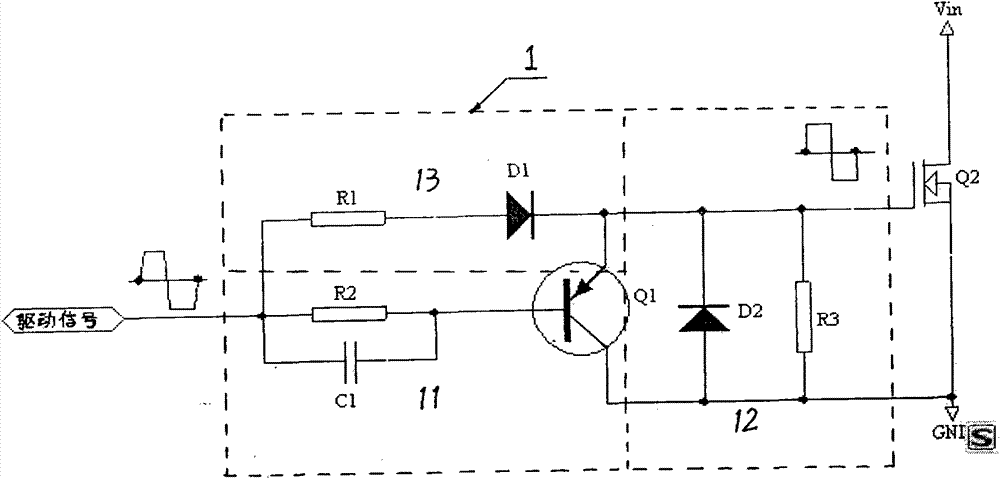
[0018] refer to figure 1 , the present embodiment includes a MOS transistor Q2 and a drive signal input end, and a drive circuit 1 is provided at the connection between the control input end of the MOS transistor Q2 and the drive signal input end; the drive circuit 1 is composed of a fast turn-off path 11, a discharge path 12 and the anti-surge impact path 13; the fast turn-off path 11 and the anti-surge impact path 13 are connected in parallel and connected between the control input terminal of the MOS transistor Q2 and the drive signal input end, and the discharge path 12 is connected across the Between the gate of the MOS transistor and the ground terminal.
[0019] In this embodiment, the drive circuit 1 is formed by connecting resistors R1-R3, diodes D1-D2, filter capacitor C1, and transistor Q1; the resistor R2 and filter capacitor C1 are connected in parallel to the base of the transistor Q1 to form a fast turn-off path 11. The resistor R1 and the diode D1 are connecte...
specific Embodiment 2
[0025] The characteristics of the specific embodiment 2 of the present invention are: the driving tube Q1 is composed of a MOS tube, the gate of the MOS tube is connected to the output terminal of the fast turn-off path 11, the source is connected to the ground terminal, and the drain is connected to the anti-wave The output terminal of the surge impact path 13 is connected; that is, the resistor R2 is connected in parallel with the filter capacitor C1 to form a fast turn-off path 11, and the resistor R1 and diode D1 are connected in series to the gate of the MOS transistor to form a fast turn-off path 11 , the resistor R1 and the diode D1 are connected in series to the drain of the MOS tube to form a surge prevention path 13, and the discharge resistor R3 is connected between the gate of the MOS switch Q2 and the ground terminal to form a discharge path 12, and the MOS switch Q2 The source of the MOS tube and the collector of the MOS tube are grounded.
specific Embodiment 3
[0026] The feature of specific embodiment 3 of the present invention is: omit figure 1 The voltage-limiting diode D2 shown is the same as that of the specific embodiment 1 or the specific embodiment 2.
PUM
 Abstract
Description
Claims
Application Information
