RET IGBT device structure with separation gate structure and manufacturing method thereof
A device structure and separation gate technology, applied in semiconductor/solid-state device manufacturing, semiconductor devices, electrical components, etc., can solve the problems of reducing blocking ability, reducing device switching speed, increasing switching loss, etc., and reducing leakage current. , the effect of reducing charging and reducing switching loss
- Summary
- Abstract
- Description
- Claims
- Application Information
AI Technical Summary
Problems solved by technology
Method used
Image


Examples
Embodiment 1
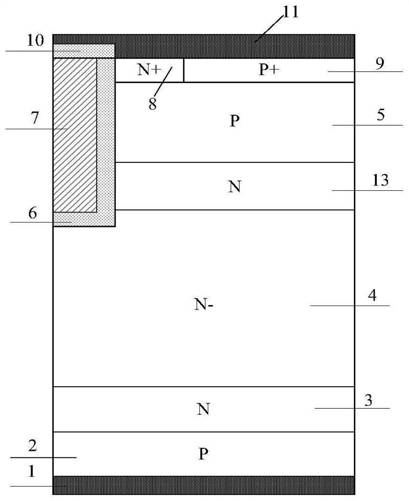
[0086] An embodiment of a RET IGBT device with a split gate structure, such as figure 2 As shown, it includes: collector metal 1, P-type collector region 2, N-type field stop layer 3 and N-drift region 4 stacked in sequence from bottom to top, and the trench gate located above N-drift region 4 structure and a trench emitter structure, the trench gate structure includes a separation gate dielectric layer 6, a separation gate electrode 17 above the separation gate dielectric layer 6, a gate dielectric layer 18 above the separation gate electrode 17, and a gate dielectric layer 18 in the gate dielectric layer 18 The polysilicon gate electrode 7 and the isolation dielectric layer 10 above the polysilicon gate electrode 7, the trench emitter structure includes a trench emitter dielectric layer 14 and a polysilicon trench emitter electrode 15 in the trench emitter dielectric layer 14;
[0087] There is an N-type buried layer 16 between the trench gate structure and the trench emitte...
Embodiment 2
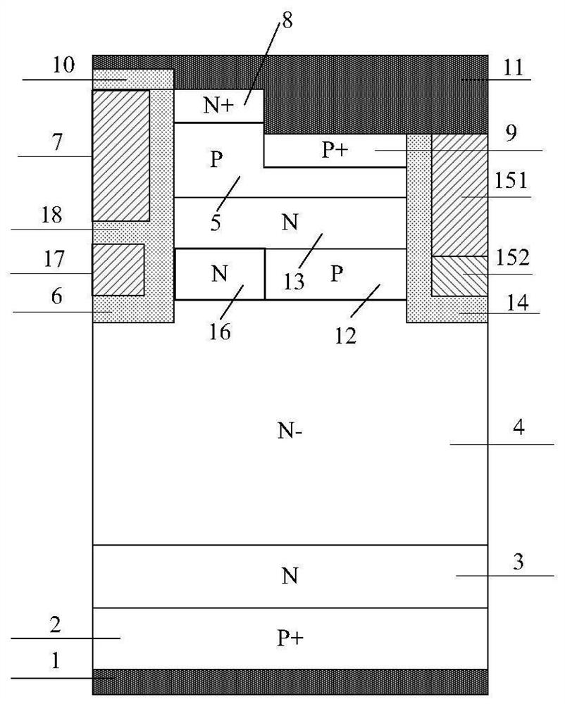
[0125] An embodiment of a RET IGBT device with a split gate structure, such as image 3 As shown, the difference between this embodiment and Embodiment 1 is that the polycrystalline trench emitter electrode 15 includes a P-type doped polysilicon electrode 151 and an N-type doped polysilicon electrode 152 below the P-type doped polysilicon electrode 151, so The doping concentration of the N-type doped polysilicon electrode 152 is less than the concentration of the P-type doped polysilicon electrode 151, the thickness of the N-type doped polysilicon electrode 152 is less than the thickness of the P-type doped polysilicon electrode 151, and the N-type Doped polysilicon is fully depleted.
[0126] By doing different doping to the polysilicon electrode of the trench emitter structure, when the device is turned off, the PN junction formed by the trench emitter is reverse-biased, and the N-type doped polysilicon electrode 152 has a lower doping concentration and a smaller thickness. ...
Embodiment 3
[0128] An embodiment of a RET IGBT device with a split gate structure, such as Figure 4As shown, the difference between this embodiment and Embodiment 1 is that the polysilicon gate electrode 7 includes a P-type doped polysilicon electrode 71, an N-type doped polysilicon electrode 72 below the P-type doped polysilicon electrode 71, and an N-type doped polysilicon electrode 72. The concentration of 72 is less than that of the P-type doped polysilicon electrode 71 , and the thickness of the N-type doped polysilicon electrode 72 is less than the thickness of the P-type doped polysilicon electrode 71 .
[0129] When the device is turned off, the PN junction in the trench gate is reverse-biased, and the N-type region is completely depleted, reducing the gate capacitance Cge.
PUM
 Abstract
Description
Claims
Application Information